
Preparation method for gold-tin eutectic solder

A tin alloy and solder technology, applied in the field of multilayer metal alloy film preparation, can solve the problems of poor control of electroplating reaction, difficulty in precise control of thickness and composition, low utilization rate of electron beam evaporation materials, etc., to achieve fast deposition rate, Guaranteed consistent effect

Active Publication Date: 2013-06-26
INST OF APPLIED ELECTRONICS CHINA ACAD OF ENG PHYSICS
View PDF4 Cites 19 Cited by
  • Summary
  • Abstract
  • Description
  • Claims
  • Application Information

AI Technical Summary

Problems solved by technology

[0005] However, there are some defects in the above-mentioned method for preparing gold-tin alloy solder, that is, the utilization rate of the electron beam evaporation material is too low and the electroplating reaction is not well controlled, and the thickness and composition are difficult to accurately control.

Method used


Image

  • Preparation method for gold-tin eutectic solder

Examples


Embodiment Construction

[0023] The present invention will be further described below in conjunction with the drawings.

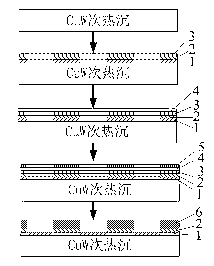
[0024] Such as figure 1 Shown is the production flow chart of the present invention. The figure is a schematic cross-sectional view of material processing, in which the CuW secondary heat sink is used as the underlying material.

[0025] Put the prepared CuW secondary heat sink into the magnetron sputtering coating machine, deposit by magnetron sputtering coating technology, and deposit the metal film on the CuW secondary heat sink successively; deposit a layer of Ti or Ni film 1 at the bottom, Deposit a layer of Pt film 2 on the Ti or Ni film 1 again, and finally deposit a layer of Au film 3 on the Pt film 2, so as to form an underlying metal film such as Ti / Pt / Au or Ni / Pt / Au. CuW secondary heat sink, the total thickness of the deposited Ti / Pt / Au or Ni / Pt / Au bottom metal film is controlled between 850~900nm.

[0026] Put the above-mentioned CuW secondary heat sink with Ti / Pt / Au or Ni / P...


PUM


Abstract

The invention discloses a preparation method for gold-tin eutectic solder. According to the method, various metal films deposit on a CuW secondary heat sink by using the Au target and Sn target layering magnetron sputtering technique, and the gold-tin eutectic solder is formed by sintering of high temperature alloy. Compared with the prior art, the preparation method for the gold-tin eutectic solder has the advantages that the deposition rate is high, uniformity of deposited layer thicknesses can be guaranteed through rotation of a base plate in deposition, and the shortcomings that use ratios are low, plating reactions are difficult to control and thicknesses and ingredients are difficult to accurately control due to a traditional method of electron beam evaporation or layered plating are overcome.

Description

Technical field [0001] The invention belongs to the technical field of preparation of multilayer metal alloy films, and specifically relates to a method for preparing gold-tin alloy solder, which is suitable for the welding of optoelectronic packaging and high-reliability military electronic devices, especially semiconductor lasers and integrated chips in the microelectronics industry. Reliability package. Background technique [0002] High-power diode laser chips (DL) have developed rapidly in recent years. Now the highest continuous laser diode chip output power in the laboratory can reach more than kilowatts, and its photoelectric efficiency can reach more than 70%. This poses a new challenge to the packaging process. How to quickly take away such a huge amount of heat and maintain the normal operation of the chip has become the primary issue of the packaging process. Gold-tin alloy solder has the characteristics of high yield strength, good thermal conductivity, and low melt...

Claims


Application Information

Patent Timeline
IPC IPC(8): B23K35/40C23C14/35C23C14/16
Inventor 王昭
Owner INST OF APPLIED ELECTRONICS CHINA ACAD OF ENG PHYSICS
Learn More