Method for controlling growth of P-type GaN low-flow dopant

A growth method and dopant technology, which is applied in the direction of single crystal growth, crystal growth, single crystal growth, etc., can solve the problems of large damage, poor electrical conductivity, and increased volume, so as to reduce production costs and improve electrical conductivity , Improve the effect of crystal quality

Inactive Publication Date: 2013-07-24
BEIJING UNIV OF TECH
View PDF4 Cites 10 Cited by
  • Summary
  • Abstract
  • Description
  • Claims
  • Application Information

AI Technical Summary

Problems solved by technology

Usually LEDs or lasers (LDs) use InGaN / GaN multiple quantum wells as the active region, and use Mg:GaN (p-GaN) material as the p-type material, and p-GaN with high conductivity requires high growth This will greatly damage the active layer InGaN in the high temperature environment for the subsequent growth of p-GaN, resulting in excessive segregation and condensation of the InGaN phase, increasing the volume of the indium-rich and indium-poor regions, and the number of radiative recombination pairs and the quantum confinement effect. Reduced, resulting in a sharp drop in luminous intensity, lowering the growth temperature will inevitably lead to a decrease in the quality of p-GaN crystals, aggravated compensation effects, worsened electrical conductivity, and increased device voltage, so how can we obtain p-GaN with high crystal quality and high hole concentration at low temperature? -What about GaN material?

Method used


Image

  • Method for controlling growth of P-type GaN low-flow dopant
  • Method for controlling growth of P-type GaN low-flow dopant
  • Method for controlling growth of P-type GaN low-flow dopant

Examples


Embodiment Construction

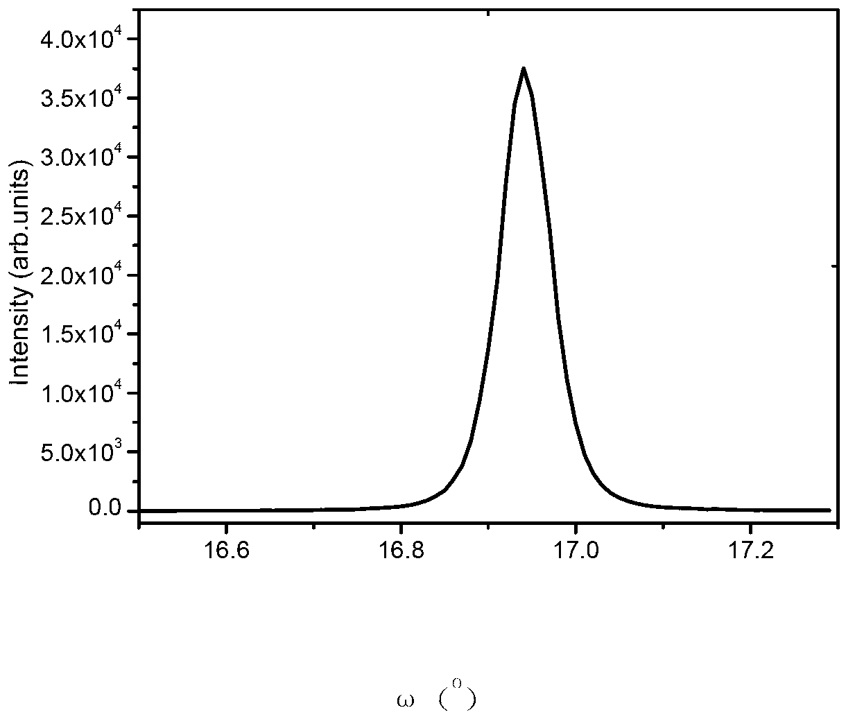
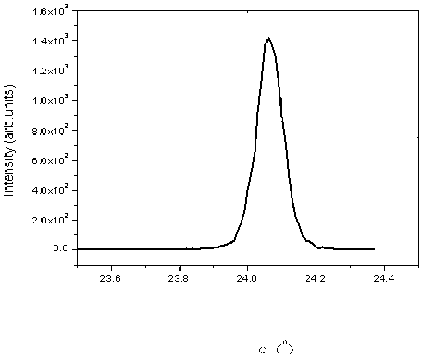
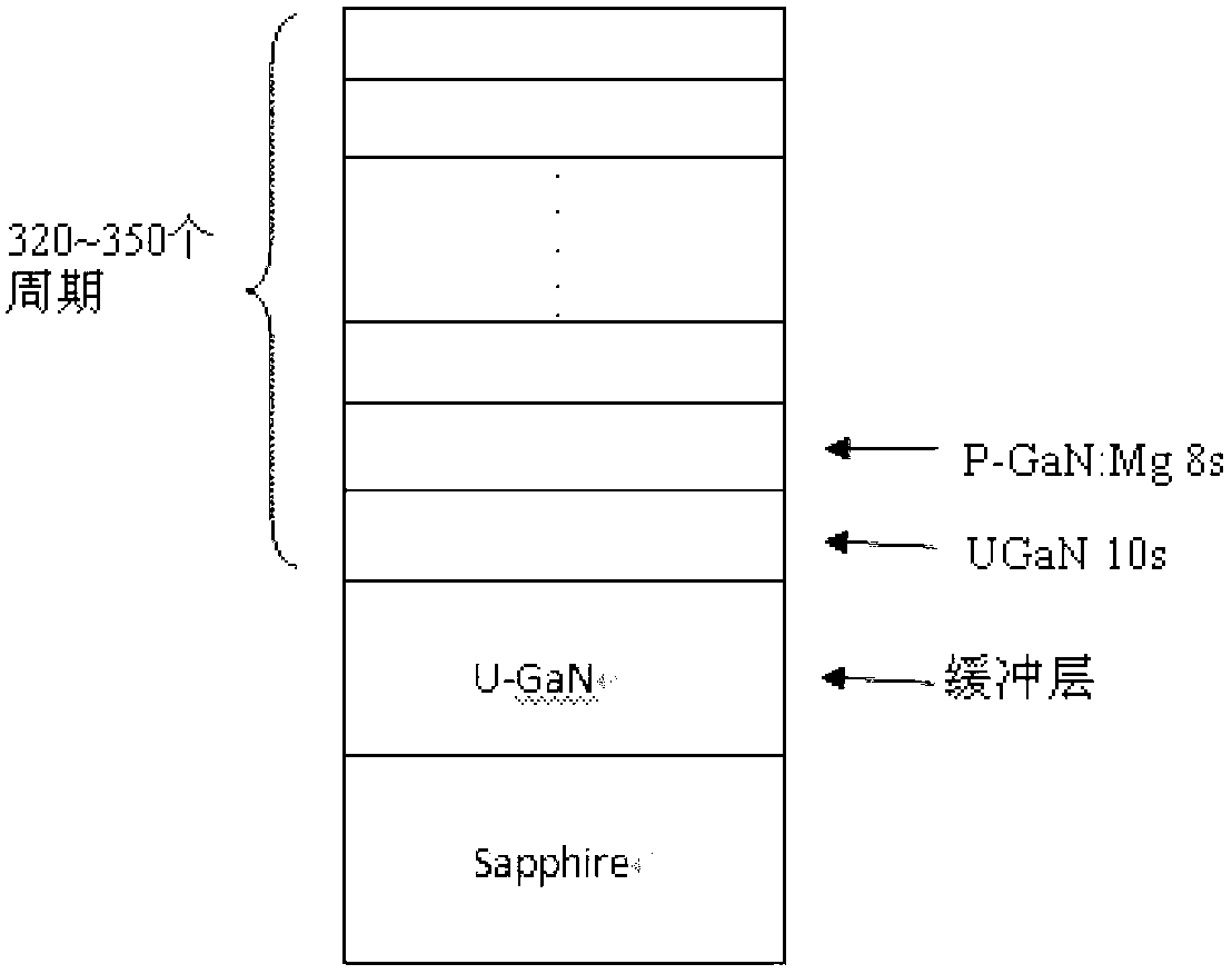
[0021] In order to make the present invention clearer, combined with figure 1 The present invention is further described in detail.

[0022] The method for growing P-type GaN material by MOCVD equipment provided by the present invention, its specific growth structure is as follows figure 1 As shown, the structure from bottom to top is: sapphire substrate, non-doped GaN buffer layer, and P-type GaN growth layer. The source materials for epitaxial growth are: TMGa and NH 3 as Ga source and N source respectively, CP 2 Mg acts as a Mg dopant. h 2 For the carrier gas. details as follows:

[0023] (1) Veeco D180 MOCVD equipment is used, and (0001) surface sapphire is selected as the substrate.

[0024] (2) Put the sapphire substrate into the MOCVD reaction chamber, 2 The chamber temperature was raised to 1100°C under atmosphere and held for three minutes to clean the substrate.

[0025] (3) Lower the temperature of the reaction chamber to 500°C, and epitaxially grow a low-t...


PUM

PropertyMeasurementUnit
thicknessaaaaaaaaaa

Abstract

The invention relates to a method for controlling the growth of a P-type GaN low-rate dopant, and belongs to the field of preparation of semiconductor materials. According to the method, a low-temperature core-forming layer, an unintentionally doped GaN layer and then a p-type GaN layer are sequentially grown upwards on a substrate with Cp2Mg as the p-type dopant, the non-doped GaN layer is grown for 10 seconds before the growth of the p-type GaN layer, then a CP2Mg source is inlet and grown for 8 seconds, and the growth is repeated for 320-350 periods with the 18 seconds as the single period; and the flow of the CP2Mg is controlled in the range of 35-50 sccm, and the growth temperature is 920-980 DEG C. Based on the method, the Mg atom intermingling efficiency is increased, the self-compensation effect of the Mg atom is restrained, the hole concentration is improved, the crystal quality is improved, and therefore the high-performance p-type GaN material is obtained; and the method provides beneficial assistance for reducing the forward voltage drop of a GaN-based LED (light-emitting device) and prolonging the service life.

Description

technical field [0001] The invention relates to the preparation of a single doping source CP on a sapphire substrate by using metal organic chemical vapor deposition (MOCVD) technology 2 A p-type GaN material of Mg belongs to the field of semiconductor material preparation. Background technique [0002] GaN is known as the third-generation semiconductor material. It has the characteristics of wide bandgap, high breakdown electric field, and high electron saturation drift speed. It is especially suitable for the preparation of a new generation of high-temperature, high-frequency, high-power and radiation-resistant electronic devices. Therefore, the application of GaN materials has high expectations from all walks of life. [0003] GaN-based products (such as LEDs) have been commercialized, but the problems in the materials limit the improvement of device performance, so the research on GaN materials is still uninterrupted, such as the research on Mg-doped p-type GaN material...

Claims


Application Information

Patent Timeline
Patent Type & Authority Applications(China)
IPC IPC(8): C30B25/02C30B29/38
Inventor 韩军邢艳辉李影智
Owner BEIJING UNIV OF TECH
Why Eureka
Try Eureka