Method of preparing groove discrete semiconductor device
A discrete device and semiconductor technology, applied in semiconductor/solid-state device manufacturing, electrical components, circuits, etc., can solve problems such as poor terminal structure, poor device breakdown voltage and reliability, and difficult to generate
- Summary
- Abstract
- Description
- Claims
- Application Information
AI Technical Summary
Problems solved by technology
Method used
Image

Examples
Embodiment 1
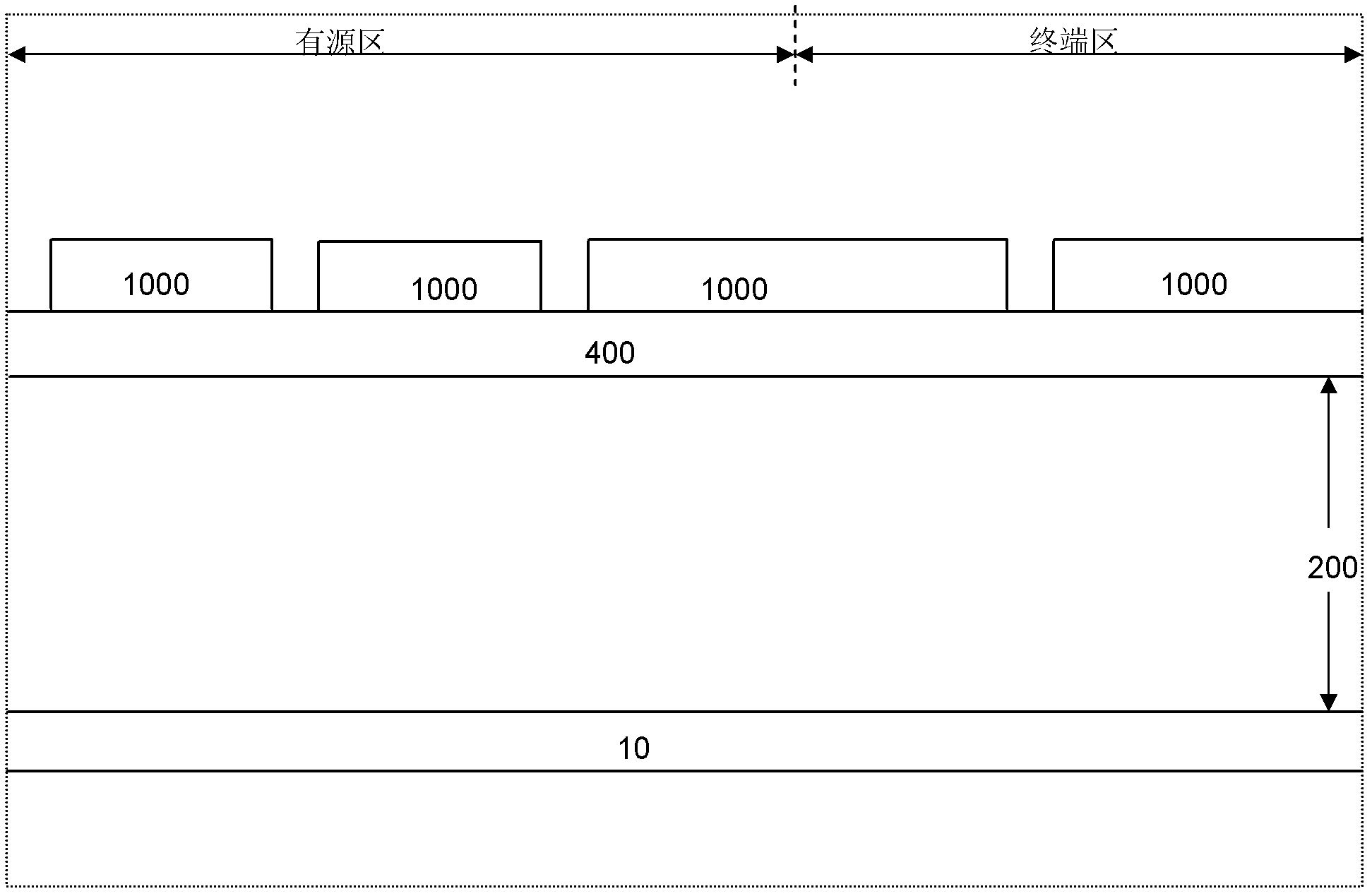
[0081] Such as figure 1 As shown, the epitaxial layer 200 is placed above the substrate 10. First, an oxide layer 400 (with a thickness of 0.3um to 1.5um oxide hard mask) is formed on the epitaxial layer by deposition or thermal growth, and then on the oxide layer A photoresist coating 1000 is deposited and then patterned through a trench mask to expose portions of the oxide layer.
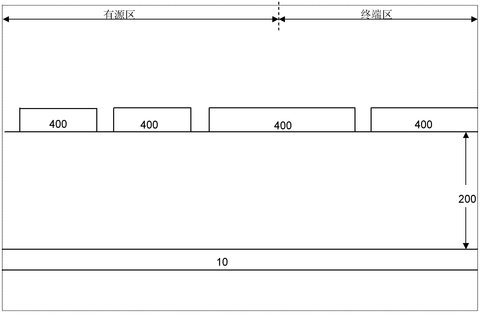
[0082] Such as figure 2 As shown, after dry etching the oxide layer exposed by patterning the trench mask, the epitaxial layer is exposed, and then the photolithographic coating is removed.
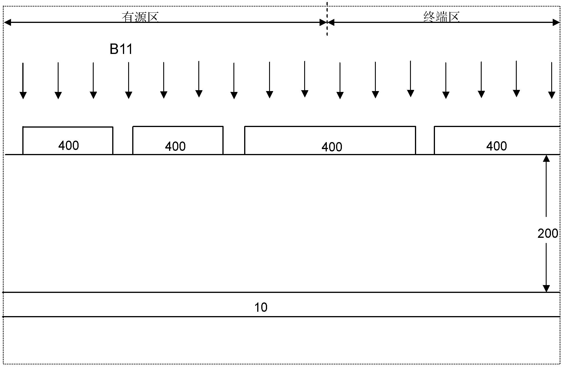
[0083] Such as image 3 As shown, implant P-type dopants on the surface of the silicon wafer (the dose is 2e12 / cm 3 to 2e14 / cm 3 ), the part covered by the original oxide layer 400 has not been implanted, the part not covered by the original oxide layer, the P-type dopant will be injected into the surface of the epitaxial layer to form a P-type region, and the P-type dopant can be B11 (boron boron ).
...
Embodiment 2
[0098] The technical scheme of the present embodiment is roughly the same as that of embodiment 1, and its difference only lies in:
[0099] In the above example 1 Figure 5 Before etching the trench, first deposit a layer of oxide layer and seal the opening width of the trench mask in the oxide layer ranging from 0.2um to 0.6um. The width of the sealed opening can be 0.2um or 0.3um or 0.4um or 0.5um or 0.6um, depending on the preparation method, the advantage of this step is that some trench mask openings are implanted with P-type dopants (P-type 1 region) but not The trench is opened, the terminal structure of the device is better, so the breakdown voltage of the device is higher and more stable, and then the oxide layer is dry-etched to remove the oxide layer on the opening and expose the epitaxial layer on the opening; After etching the trench, only those openings that are not sealed by the precipitated oxide layer are opened. The trench (1.0um to 7.0um in depth and 0.2um...
Embodiment 3
[0101] The technical scheme of the present embodiment is roughly the same as that of embodiment 1, and its difference only lies in:
[0102] In the above example 1 Figure 15 Before etching the contact hole trench, first deposit a layer of (LPCVD) oxide layer, and then dry-etch the oxide layer to remove the oxide layer in the opening of the contact hole trench, exposing the epitaxial layer in the opening; etched contact hole trenches. Other steps are basically identical with embodiment 1, and the cross section of device is as follows Figure 19 shown.
PUM
| Property | Measurement | Unit |
|---|---|---|
| Thickness | aaaaa | aaaaa |
| Thickness | aaaaa | aaaaa |
| Thickness | aaaaa | aaaaa |
Abstract
Description
Claims
Application Information
 - R&D
- Intellectual Property
- Life Sciences
- Materials
- Tech Scout
- Unparalleled Data Quality
- Higher Quality Content
- 60% Fewer Hallucinations
Browse by: Latest US Patents, China's latest patents, Technical Efficacy Thesaurus, Application Domain, Technology Topic, Popular Technical Reports.
© 2025 PatSnap. All rights reserved.Legal|Privacy policy|Modern Slavery Act Transparency Statement|Sitemap|About US| Contact US: help@patsnap.com