
Grapheme nanometer stripe field-effect tube of three-material heterogeneous grid structure

A nano-strip and field-effect tube technology, which is applied in the field of structural optimization of device performance, can solve problems such as device performance degradation, and achieve the effects of large drive current, enhanced capacity, and suppression of short-channel effects

Inactive Publication Date: 2013-08-21
NANJING UNIV OF POSTS & TELECOMM
View PDF3 Cites 5 Cited by
  • Summary
  • Abstract
  • Description
  • Claims
  • Application Information

AI Technical Summary

Problems solved by technology

[0007] Technical problem: the purpose of the present invention is to solve the bipolar effect that traditional graphene nanostrip field effect transistors will have, and as the size of the device continues to shrink, there will be a short channel effect that will cause a decline in device performance. The advantages of the mass gate device, three metals with different work functions are used for the gate to form the heterogeneous gate of the MOS, and a graphene nanostrip field effect transistor with a three-material heterogeneous gate structure is proposed

Method used


Image

  • Grapheme nanometer stripe field-effect tube of three-material heterogeneous grid structure
  • Grapheme nanometer stripe field-effect tube of three-material heterogeneous grid structure
  • Grapheme nanometer stripe field-effect tube of three-material heterogeneous grid structure

Examples


Embodiment Construction

[0014] The idea of ​​the present invention will be further described in detail below in conjunction with the accompanying drawings.

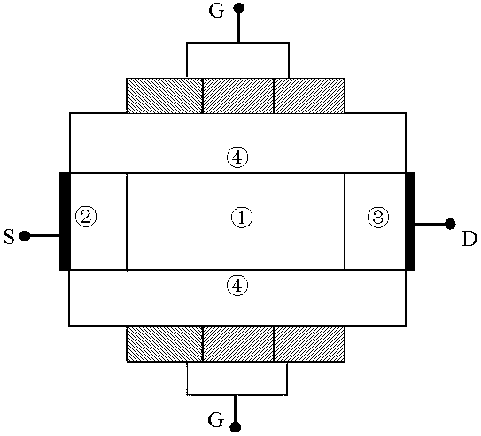
[0015] Such as figure 1 As shown, the conductive channel 1, the source region 2 and the drain region 3 are all made of graphene nano-strip material, and a fundamental semiconductor graphene nano-strip is selected, and the middle part is used as a graphene with a three-material heterogeneous gate structure. The conductive channel 1 of the nanostrip field effect tube, after the two ends of the intrinsic semiconductor graphene nanostrips are N-type heavily doped with molecules or metal ions, they are respectively used as graphene nanostrips with a three-material heterogeneous gate structure The source region 2 and the drain region 3 of the field effect transistor; outside the conductive channel 1, the source region 2 and the drain region 3, a layer of gate oxide layer 4 is formed by atomic deposition and other methods, and re-precipitated outside t...


PUM


Abstract

The invention discloses a grapheme nanometer stripe field-effect tube of a three-material heterogeneous grid structure. A conducting channel (1), a source region (2) and a drain region (3) of the field-effect tube are all made of grapheme nanometer stripe materials. Besides the conducting channel (1), the source region (2) and the drain region (3), a grid oxide layer (4) is generated by methods of atomic deposition and the like, a metal electrode layer is reprecipitated outside the grid oxide layer (4) to serve as a grid (G) of the grapheme nanometer stripe field-effect tube of the three-material heterogeneous grid structure, and the grid (G) is made of conducting metal with three different work functions to form the heterogeneous grid of the grapheme nanometer stripe field-effect tube of the three-material heterogeneous grid structure. When the work functions of three materials gradually decrease from a source to a drain, or when a middle work function is the maximum and a work function close to the side of the drain is minimum, the structure can effectively improve performance, and the field-effect tube has lower leakage currents and a higher current switching ratio, and can suppress a drain induced barrier lowering (DIBL) effect.

Description

technical field [0001] The invention relates to the field of graphene nano-ribbon field effect tubes, in particular to the optimization of the structure of the graphene nano-ribbon device to the performance of the device. Background technique [0002] Graphene is a planar material consisting of carbon atoms through sp 2 It is composed of chemical bonds to form a honeycomb arrangement, and it is the only planar material found so far that maintains a stable two-dimensional structure at room temperature. At present, silicon nano-devices have almost reached their limits, and it is difficult to further improve their performance. Thanks to its high carrier mobility, excellent mechanical properties and thermal stability, graphene can well overcome the limitations of silicon material devices when their performance is further improved, and is considered to be the Materials that can replace silicon-based devices in the future. [0003] Graphene nanoribbons can be formed by etching ...

Claims


Application Information

Patent Timeline
Patent Type & Authority Applications(China)
IPC IPC(8): H01L29/786H01L29/49B82Y10/00
Inventor 王伟夏春萍肖广然杨晓
Owner NANJING UNIV OF POSTS & TELECOMM
Learn More