Method for preparing core-shell organic/cadmium sulfide nanowire heterojunction arrays

An organic nanowire and nanotube array technology, which is applied in the preparation field of core-shell organic cadmium sulfide semiconductor nanowire heterojunction and cadmium sulfide nanotube array, can solve the problem of organic nanowire crystal quality damage, poor controllability, and difficulty in problems of precise control

Inactive Publication Date: 2013-08-21
SUZHOU UNIV
View PDF2 Cites 13 Cited by
  • Summary
  • Abstract
  • Description
  • Claims
  • Application Information

AI Technical Summary

Problems solved by technology

However, the synthesis method mentioned above is limited by the size of the AAO template, the yield is low, and the alumina template must be dissolved in further application. The introduction of organic solvents will inevitably damage the crystal quality of organic nanowires. This method Poor controllability, it is difficult to precisely control the structure of organic / inorganic heterojunction nanowires

Method used


Image

  • Method for preparing core-shell organic/cadmium sulfide nanowire heterojunction arrays
  • Method for preparing core-shell organic/cadmium sulfide nanowire heterojunction arrays
  • Method for preparing core-shell organic/cadmium sulfide nanowire heterojunction arrays

Examples


Embodiment 1

[0042] Example 1: Preparation of CdS-CuPc heterojunction nanowires

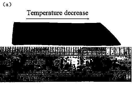
[0043] A 6nm gold thin film was deposited on a silicon substrate by electron beam evaporation, and copper phthalocyanine nanowire arrays were grown by physical vapor deposition. Concrete growth parameter is as follows: according to the flowing direction of airflow, the porcelain boat that copper phthalocyanine powder is housed is put into the high-temperature zone of vacuum tube furnace; The center of the temperature zone is about 10-20cm; start the mechanical pump to evacuate, so that the vacuum degree in the furnace chamber of the vacuum tube furnace is below 1Pa, and then pass into the inert gas in the quartz tube, and the gas flow rate is 30-60sccm; when the quartz tube When the medium is completely in an inert gas atmosphere, while maintaining the inert gas inflow; control the tube furnace to increase the temperature to 415 °C at a rate of 20 °C / min, and then keep the temperature for 30 min to fully proc...

Embodiment 2

[0048] Example 2: Preparation of CdS-PTCDA heterojunction nanowires

[0049] Perylenetetracarboxylic dianhydride nanowire arrays were grown by physical vapor deposition. The specific growth parameters are as follows: according to the flow direction of the air flow, a porcelain boat containing an appropriate amount of perylenetetracarboxylic dianhydride powder is placed in the high temperature zone of the vacuum tube furnace; and the cleaned silicon substrate is placed in the low temperature zone of the vacuum tube furnace. Zone, about 10-20cm away from the center of the temperature zone; start the mechanical pump to evacuate, so that the vacuum degree in the furnace chamber of the vacuum tube furnace is below 1Pa, and then pass inert gas into the quartz tube, and the gas flow rate is 30-60sccm; When the quartz tube is completely in an inert gas atmosphere, while keeping the inert gas flowing in, control the tube furnace to raise the temperature to 415°C at a rate of 20°C / min, ...


PUM

PropertyMeasurementUnit
lengthaaaaaaaaaa

Abstract

The invention discloses a method for preparing core-shell organic cadmium sulfide semiconductor nanowire heterojunctions and cadmium sulfide nanotubes. The method includes the steps that a single crystal organic nanowire array is grown through physical vapor deposition, the high-density organic nanowire array is used as a template, and a cadmium sulfide (CdS) shell layer is grown on a nanowire surface layer in a wrapping mode through atomic layer deposition (ALD); controllable preparation of different types of core-shell organic or inorganic heterojunction nano-structure arrays can be conveniently achieved through control over types of organic nanowires and technological conditions of atomic layer deposition; meanwhile, the organic nanowires in core shells are evaporated by being heated, and corresponding hollow inorganic nanotube arrays can be obtained. The method is easy to operate and simple in technology, products are even and high in controllability, and formation of the heterojunction can be controlled in an atomic layer grade; the heterojunction nanowires and the nanotube arrays prepared through the method have broad application prospects in nanoelectronics and photoelectron fields such as solar cells, photoswitches and sensors.

Description

technical field [0001] The invention relates to the field of semiconductor nanomaterials and their heterojunction preparation, in particular to a method for preparing a core-shell organic cadmium sulfide semiconductor nanowire heterojunction and a cadmium sulfide nanotube array. Background technique [0002] Semiconductor heterojunctions are fundamental units in a variety of optoelectronic devices and have broad and important applications. Heterojunctions can be divided into homogeneous (p-p or n-n) and heterogeneous (p-n) heterojunctions. The traditional semiconductor heterojunction is composed of two or more single crystal semiconductors with different band gaps or conductivity types due to composition modulation. It can be designed to have p-n, p-n-p, n-p-n, p-i-n or p-i-p according to needs. heterogeneous structure. The rapid development of information technology has higher and higher requirements for the miniaturization and integration of electronic and optoelectronic...

Claims


Application Information

Patent Timeline
Patent Type & Authority Applications(China)
IPC IPC(8): H01L51/56
Inventor 揭建胜吴艺明张希威张玉萍张晓珍卞良
Owner SUZHOU UNIV
Why Eureka
Try Eureka