Electroluminescent diode device

A luminescence and diode technology, which is applied in the field of organic ultraviolet electroluminescent diode devices, can solve the problems such as no light-emitting diode devices have been found, and achieve the effects of reduced starting voltage, improved electro-optical conversion efficiency, and reduced power consumption

Active Publication Date: 2013-09-25
TCL CHINA STAR OPTOELECTRONICS TECH CO LTD
View PDF3 Cites 10 Cited by
  • Summary
  • Abstract
  • Description
  • Claims
  • Application Information

AI Technical Summary

Problems solved by technology

Before the 1950s, mercury lamps were the only artificial ultraviolet light sources, but they were not used in practice
At present, there are no relevant reports on organic ultraviolet electroluminescent diode devices based on flexible substrates.

Method used


Image

  • Electroluminescent diode device
  • Electroluminescent diode device
  • Electroluminescent diode device

Examples


Embodiment 1

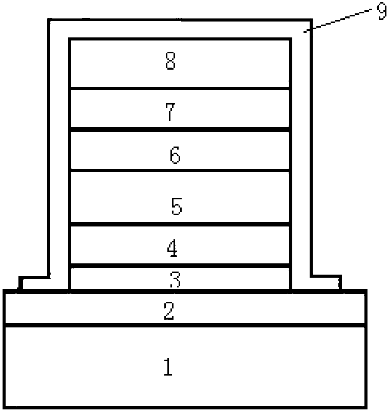
[0044] The structure of the electroluminescent device of the present invention is as figure 1 As shown, from bottom to top includes: It includes:

[0045] A transparent flexible substrate, at least one selected from polymethyl methacrylate, polyethylene adipate or polycarbonate;

[0046] The first protective layer, which is a barix layer, is composed of alternate laminations of organic polymer materials and inorganic materials; since the materials of the first protective layer need to be able to transmit ultraviolet light, the organic polymer materials can be selectively polymerized Methyl methacrylate, polyethylene adipate or polycarbonate, etc., the inorganic material can be selected from materials with a band gap not smaller than the optical band gap of 3.96eV silicon nitride, such as aluminum nitride, silicon nitride , silicon oxide, etc. Silicon nitride is a commonly used light-transmitting medium for ultraviolet devices;

[0047] an anode, which is an ITO layer;

[0...

Embodiment 2

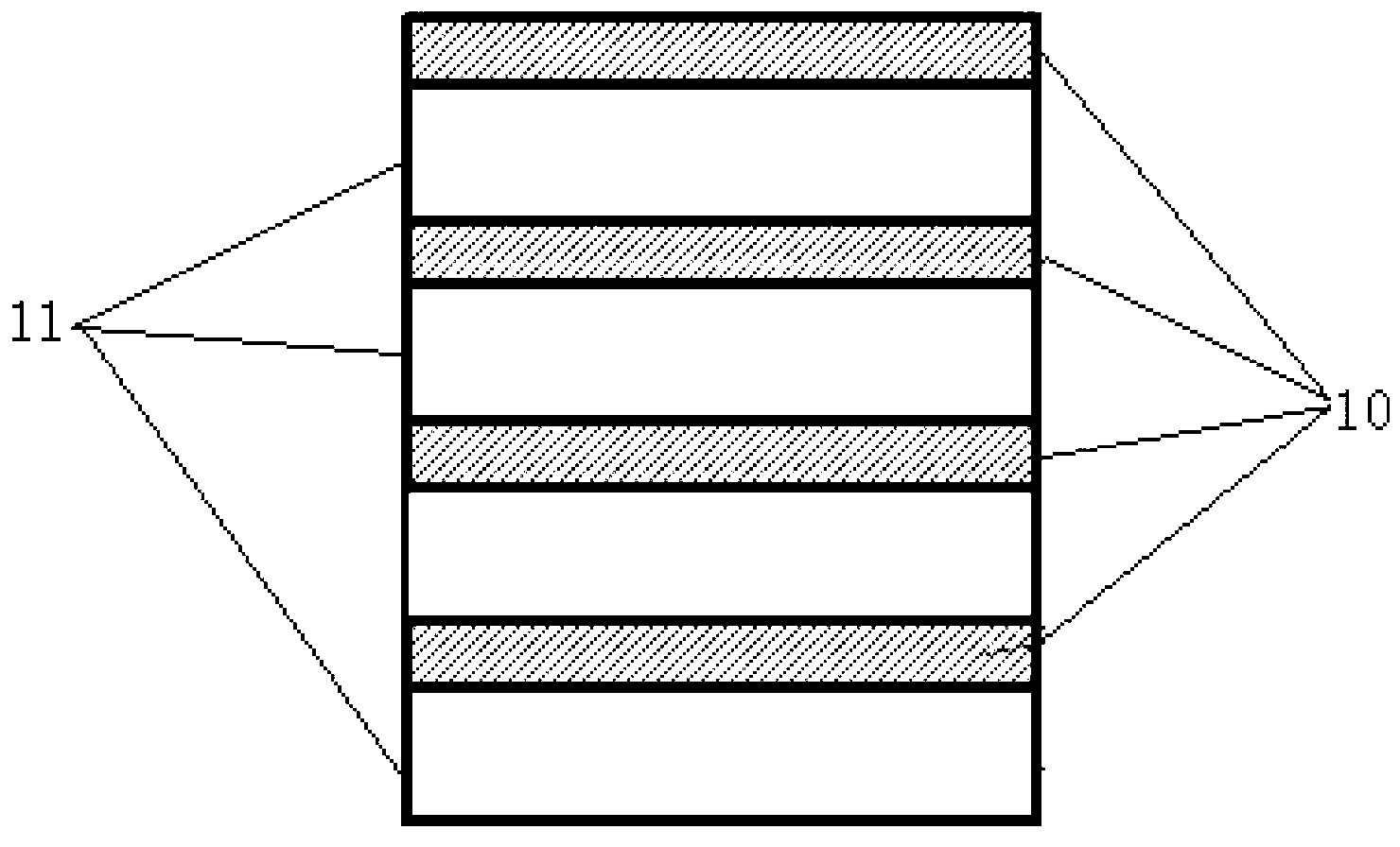
[0061] Such as image 3 As shown, the structure of another electroluminescent diode of the present invention also includes on the basis of the structure disclosed in embodiment 1:

[0062] An encapsulation cover plate, including a flexible cover plate, a third protective layer and a desiccant layer arranged in sequence;

[0063] The structure of the third protective layer is composed of organic polymer materials or alternately stacked organic polymer materials and inorganic materials;

[0064] Wherein, the encapsulation cover plate and the electroluminescent diode are packaged at intervals relative to the outside of the second protective layer in the direction in which the desiccant layer and the electroluminescent diode are arranged in sequence.

[0065] The third protective layer is a Barix layer, and the polymer layer material it includes can be at least one of the organic polymer materials selected from the following substances: parylene, polychlorinated p-xylylene, polye...


PUM


Abstract

The invention relates to an electroluminescent diode device which comprises a transparent flexible substrate, a first protecting layer, an anode, a hole transporting layer, an ultraviolet light emission layer, a hole barrier layer, an electron transporting layer and a cathode, wherein the first protecting layer, the anode, the hole transporting layer, the ultraviolet light emission layer, the hole barrier layer, the electron transporting layer and the cathode are sequentially arranged on the flexible substrate. An ultraviolet light material contained by the ultraviolet light emission layer is selected from at least one of a fluorene containing type material, a triphenylamine type material and a quinquephenyl type material.

Description

technical field [0001] The invention relates to the field of electroluminescent diode devices, in particular to an electroluminescent diode device, and more specifically to an organic ultraviolet electroluminescent diode device based on a flexible substrate and its application. Background technique [0002] Ultraviolet light is a general term for radiation with wavelengths from 10nm to 400nm in the electromagnetic spectrum, which cannot cause people's vision. Ultraviolet light source is a non-illumination electric light source whose main purpose is to generate ultraviolet radiation. It has fluorescence effect, biological effect, photochemical effect and photoelectric effect, and is suitable for industry, agriculture, national defense and medical treatment. The ultraviolet light source has the fluorescence effect, biological effect and photochemical effect of ultraviolet light, and is widely used in the fields of industry, agriculture, national defense and medical treatment. ...

Claims


Application Information

Patent Timeline
Patent Type & Authority Applications(China)
IPC IPC(8): H01L51/50H01L51/52H01L51/54
CPCC09K11/06C09K2211/1011C09K2211/1029Y02E10/549H10K85/6572H10K50/858H10K50/11H10K2102/311H10K77/111H10K50/15H10K50/16H10K50/18H10K50/81H10K50/82H10K50/8426H10K50/8445H10K85/60H10K85/111H10K85/141H10K2102/00
Inventor 刘亚伟
Owner TCL CHINA STAR OPTOELECTRONICS TECH CO LTD
Why Eureka
Try Eureka