Efficient and low-cost preparing method for large-area graphical sapphire substrate

A patterned sapphire, low-cost technology, used in semiconductor devices, electrical components, circuits, etc., can solve problems such as slow exposure speed, limitations, and limitations of lithography technology, and achieve simple and easy process, low cost, and simple process. Effect

Inactive Publication Date: 2013-10-02
HARBIN INST OF TECH SHENZHEN GRADUATE SCHOOL
View PDF3 Cites 13 Cited by
  • Summary
  • Abstract
  • Description
  • Claims
  • Application Information

AI Technical Summary

Problems solved by technology

However, due to the contradiction between resolution and depth of focus, there is a limit to lithography technology
Lithography based on particle focusing, whether it is ion beam lithography or electron beam lithography, although it has a high enough resolution and can obtain a relatively large exposure field of view by moving the workpiece stage, the slow exposure speed limits Applications in low-cost, high-volume production manufacturing processes

Method used


Image

  • Efficient and low-cost preparing method for large-area graphical sapphire substrate
  • Efficient and low-cost preparing method for large-area graphical sapphire substrate
  • Efficient and low-cost preparing method for large-area graphical sapphire substrate

Examples


Embodiment 1

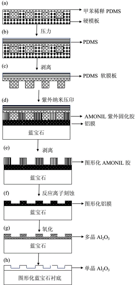
[0051] Prepare a patterned sapphire substrate for nitride epitaxial growth in the following order:

[0052] (1) Firstly, FDTS release agent is evaporated on the template of the grating structure pattern, and then the PDMS is diluted with toluene (toluene) at a concentration of 60%wt, stirred evenly, poured into a medical syringe, and then the diluted PDMS is injected into the grating structure pattern In the template, and cover the entire surface of the grating pattern structure template, and then spin the glue on the glue homogenizer: first, rotate the glue at a low speed of 900 rpm for 6 seconds, and then at a high speed of 3000 rpm, rotate the glue for 20 seconds.

[0053] (2) Prepare the PDMS prepolymer with PDMS prepolymer: curing agent = 1:10, stir evenly, and coat it on PDMS with a mass fraction of 60%wt, and then press the PDMS plate of 80μm to 120μm on the PDMS On the prepolymer, place the template on a hot plate, set the temperature of the hot plate to 90°C, cure for...

Embodiment 2

[0062] Prepare a patterned sapphire substrate for nitride epitaxial growth in the following order:

[0063] (1) Firstly, FDTS release agent is evaporated on the template of the grating structure pattern, and then PDMS is diluted with toluene, the mass concentration is 60%wt, stirred evenly, poured into a medical syringe, and then the diluted PDMS is injected into the template of the grating structure pattern and cover the entire surface of the grating graphic structure template, and then spin the glue on the glue spreader: at a low speed of 900 rpm, rotate the glue for 6 seconds, and at a high speed of 3000 rpm, rotate the glue for 20 seconds.

[0064] (2) Prepare the PDMS prepolymer with PDMS prepolymer: curing agent = 1:10, stir evenly, and coat it on 60%wt PDMS, then press the thick elastic PDMS plate on the PDMS prepolymer, Place the template on a hot plate, set the temperature of the hot plate to 90°C, solidify for 2-3 h, and cool naturally.

[0065] (3) Use tweezers to ...

Embodiment 3

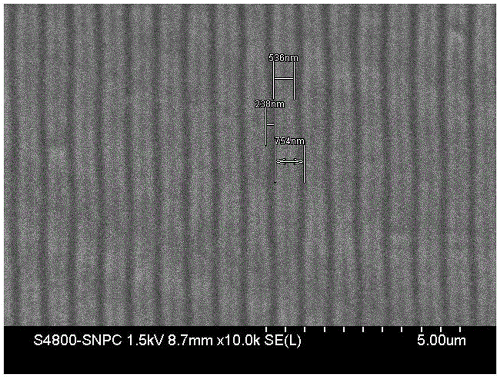
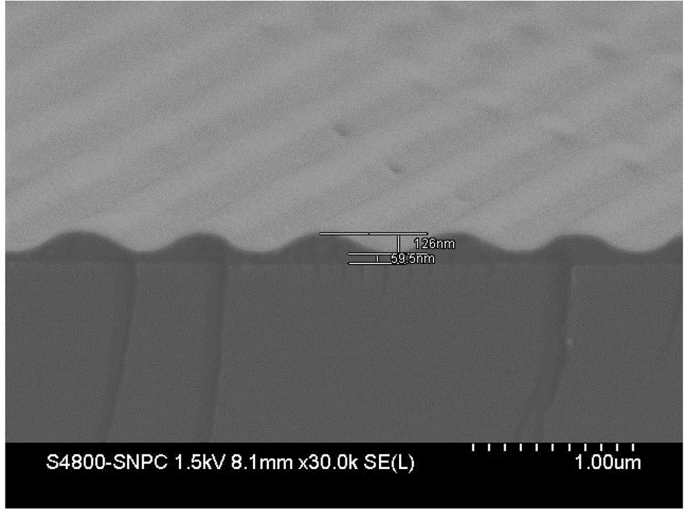
[0073] Crystal Structure Testing

[0074] The crystal structure of the prepared patterned sapphire substrate was tested by high-resolution X-ray diffractometer. Image 6 is the scan result of the patterned sapphire substrate (11-23), Figure 7 It is the XRD-ω / 2θ scanning result of the patterned sapphire substrate (0006), and the result shows that the diffraction peak width at half maximum of the patterned sapphire substrate (0006) is FWHM=0.0101°. Figure 8 It is the XRD-ω / 2θ scanning result of the unpatterned sapphire substrate (0006), and the result shows that the half maximum width of the diffraction peak of the unpatterned sapphire substrate (0006) is FWHM=0.0133°. Image 6 The XRD-Φ scanning result of the patterned sapphire substrate (11-23), the crystal plane angle between (11-23) and (0006) is φ=61.2°, and the sample is scanned from 0 to 360° around the surface normal n . exist Image 6 There are 6 diffraction peaks at equal intervals, and the difference between a...


PUM

PropertyMeasurementUnit
thicknessaaaaaaaaaa
thicknessaaaaaaaaaa
widthaaaaaaaaaa

Abstract

The invention provides an efficient and low-cost preparing method for a large-area graphical sapphire substrate, which includes the following steps: step A, coating PDMS (polydimethylsiloxane) diluted by methylbenzene in a grating structured graph hard template in a spinning manner; step B, coating a PDMS prepolymer with the PDMS diluted by methylbenzene; step C, demoulding, and obtaining a PDMS soft embossing template; step D, performing metallic aluminium film magnetron sputtering to one surface of a sapphire substrate; step E, demoulding, and obtaining an ultraviolet curing glue graph; step F, taking the graphic ultraviolet curing glue on the metallic aluminium film as a mask; step G, performing low-temperature thermal treatment, and completely oxidizing the graphic metallic aluminium film to form a graphic polycrystal Al2O3 film; step H, performing high-temperature thermal treatment to the obtained graphic polycrystal Al2O3 film, and obtaining the graphical sapphire substrate. The graphical sapphire substrate for epitaxial growth of nitride, obtained through adopting the method, has the advantages that the process is simple and feasible, the production efficiency is high, the cost is low and the area is big.

Description

technical field [0001] The invention relates to a method for preparing a patterned sapphire substrate, in particular to a method for preparing a patterned sapphire substrate with high production efficiency, low cost and large area for nitride extension growth. Background technique [0002] In recent years, high-brightness and high-power nitride light-emitting diodes (LEDs) have attracted much attention, and they are widely used in traffic lights, LCD backlights, solid-state lighting, and full-color display screens. These commercial products require LEDs to have excellent performance in terms of luminance and luminous efficiency. Sapphire has the advantages of stable chemical and physical properties, good light transmission, and reasonable cost, so it is widely used in nitride epitaxial substrates. However, due to the huge difference in lattice constant mismatch and thermal expansion coefficient mismatch between the nitride epitaxial film and the sapphire substrate at the bo...

Claims


Application Information

Patent Timeline
Patent Type & Authority Applications(China)
IPC IPC(8): H01L33/20H01L33/00
Inventor 张化宇汪桂根崔林韩杰才
Owner HARBIN INST OF TECH SHENZHEN GRADUATE SCHOOL
Why Eureka
Try Eureka