Method for preparing low-boron-doped high-conductivity hydrogenated amorphous silicon film

A hydrogenated amorphous silicon, high-conductivity technology, applied in semiconductor/solid-state device manufacturing, circuits, electrical components, etc., can solve the problems of increasing the preparation cost of hydrogenated amorphous silicon thin films, relying on the initial structure of the thin film, etc. The effect of low deposition temperature and simple preparation process

Inactive Publication Date: 2013-10-09
NINGBO INST OF MATERIALS TECH & ENG CHINESE ACADEMY OF SCI
View PDF2 Cites 6 Cited by
  • Summary
  • Abstract
  • Description
  • Claims
  • Application Information

AI Technical Summary

Problems solved by technology

Subsequent annealing is one of the effective ways to break B---H-Si bonds, but this method depends on the initial structure of the film, and subsequent annealing will increase the preparation cost of hydrogenated amorphous silicon films

Method used


Image

  • Method for preparing low-boron-doped high-conductivity hydrogenated amorphous silicon film
  • Method for preparing low-boron-doped high-conductivity hydrogenated amorphous silicon film
  • Method for preparing low-boron-doped high-conductivity hydrogenated amorphous silicon film

Examples


Embodiment 1

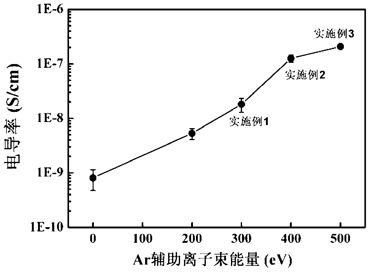
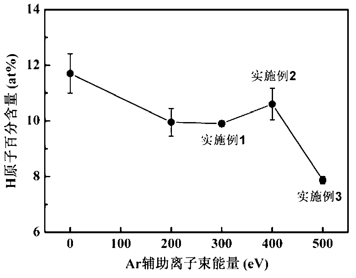
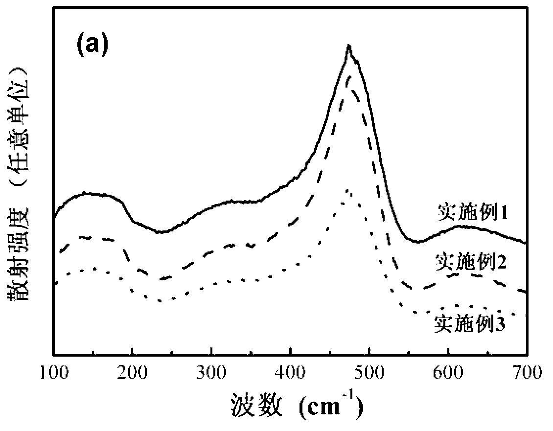
[0023] Example 1: Using ion beam assisted magnetron sputtering technology, sputtering with single crystal silicon with a boron atom doping amount of 0.1at% as a magnetron sputtering target, the background vacuum is 10 -5 Pa, the RF power is 150W, the sputtering gas is a mixed gas of argon and hydrogen, the flow ratio of argon and hydrogen in the mixed gas is 3:2, the total pressure of the sputtering gas is 0.15Pa, and the substrate temperature is 350°C , using high-purity argon as the auxiliary ion source to form an argon-assisted ion beam. The energy of the argon-assisted ion beam is 300eV, and the beam current is 15mA. The argon-assisted ion beam hits the film while sputtering and depositing the film on the surface of the quartz glass substrate. On the surface, a-Si:H hydrogenated amorphous silicon film with high conductivity under low boron doping was obtained. After testing, the thickness of the film is 160nm, and the conductivity is (1.8±0.5)×10 -8 S cm -1 , H atom cont...

Embodiment 2

[0024] Embodiment 2: Using ion beam assisted magnetron sputtering technology, sputtering with single crystal silicon with a boron atom doping amount of 0.1 at% as a magnetron sputtering target material, the background vacuum degree is 10 -5 Pa, the RF power is 200W, the sputtering gas is a mixed gas of argon and hydrogen, the flow ratio of argon and hydrogen in the mixed gas is 3:2, the total pressure of the sputtering gas is 0.2Pa, and the substrate temperature is 300°C , using high-purity argon as the auxiliary ion source to form an argon-assisted ion beam. The energy of the argon-assisted ion beam is 400eV, and the beam current is 15mA. The argon-assisted ion beam hits the film while sputtering and depositing the film on the surface of the quartz glass substrate. On the surface, a-Si:H hydrogenated amorphous silicon film with high conductivity under low boron doping was obtained. After testing, the thickness of the film is 147nm, and the conductivity is (1.3±0.2)×10 -7 S c...

Embodiment 3

[0025] Embodiment 3: Using ion beam assisted magnetron sputtering technology, sputtering with single crystal silicon with a boron atom doping amount of 0.1at% as a magnetron sputtering target material, the background vacuum degree is 10 -5 Pa, the RF power is 250W, the sputtering gas is a mixed gas of argon and hydrogen, the flow ratio of argon and hydrogen in the mixed gas is 3:2, the total pressure of the sputtering gas is 0.25Pa, and the substrate temperature is 250°C , using high-purity argon as the auxiliary ion source to form an argon-assisted ion beam. The energy of the argon-assisted ion beam is 500eV, and the beam current is 15mA. The argon-assisted ion beam hits the film while sputtering and depositing the film on the surface of the quartz glass substrate. On the surface, a-Si:H hydrogenated amorphous silicon film with high conductivity under low boron doping was obtained. After testing, the thickness of the film is 129nm, and the conductivity is (2.1±0.2)×10 -7 S c...


PUM

PropertyMeasurementUnit
thicknessaaaaaaaaaa
thicknessaaaaaaaaaa
thicknessaaaaaaaaaa

Abstract

The invention discloses a method for preparing a low-boron-doped high-conductivity hydrogenated amorphous silicon film. An ion beam auxiliary magnetic control sputtering technology is adopted, boron-doped monocrystalline silicon doped with 0.02-0.2at% of boron atoms is used as magnetic control sputtering target materials for carrying out sputtering, the base pressure is 104-105Pa, the radio frequency power is 100-300W, the sputtering gas is mixed gas of argon and hydrogen, the total pressure of the sputtering gas is 0.1-0.5Pa, the temperature of a substrate is 100-400 DEG C, the high-purity argon is used as an auxiliary atom source for forming an argon auxiliary ion beam, the energy of the argon auxiliary ion beam is 100-800eV, the beam stream is 5-30mA, the film is formed and deposited on the surface of the substrate in a sputtering mode, meanwhile, the argon auxiliary ion beam strikes the surface of the film, and the low-boron-doped high-conductivity a-Si:H hydrogenated amorphous silicon film is obtained. The method is simple in preparation process, low in cost and suitable for large-scale industrial production. The a-Si:H film prepared by the method has high conductivity and good structural characteristics, the requirements of silicon-based film solar cell window layer materials are met, and the improvement of the performance of a solar cell is facilitated.

Description

technical field [0001] The invention relates to a method for preparing a hydrogenated amorphous silicon film, in particular to a method for preparing a hydrogenated amorphous silicon film with low boron doping and high conductivity. Background technique [0002] As the window layer material of silicon-based thin-film solar cells, boron-doped hydrogenated amorphous silicon (a-Si:H) thin films with high conductivity and low light absorption are crucial for high-performance solar cells. In the disordered network structure of a-Si:H film, boron can not only be in four-coordination, which has electrical activity, but also can be in three-coordination with the formation of B---H-Si bond. At this time, the boron atom is replaced by hydrogen Atomic passivation, boron is not electrically active. Since the energy of the three-coordinated state is lower than that of the four-coordinated state, most boron is not electrically active, so the doping efficiency of boron in a-Si:H thin film...

Claims


Application Information

Patent Timeline
Patent Type & Authority Applications(China)
IPC IPC(8): H01L21/203H01L31/20C23C14/35
CPCY02P70/50
Inventor 王维燕王林青黄金华黄俊俊曾俞衡宋伟杰谭瑞琴
Owner NINGBO INST OF MATERIALS TECH & ENG CHINESE ACADEMY OF SCI
Why Eureka
Try Eureka