Method for decreasing critical size of copper-connection groove

A trench, interconnect trench technology, applied in electrical components, semiconductor/solid-state device manufacturing, circuits, etc., can solve problems such as high cost, poor resolution, and large window patterns

Inactive Publication Date: 2013-10-09
SHANGHAI HUALI MICROELECTRONICS CORP
View PDF7 Cites 8 Cited by
  • Summary
  • Abstract
  • Description
  • Claims
  • Application Information

AI Technical Summary

Problems solved by technology

However, this invention uses photolithography to form windows and then etch grooves. Due to the poor resolution of traditional photolithography machines, the window pattern after exposure and development is

Method used


Image

  • Method for decreasing critical size of copper-connection groove
  • Method for decreasing critical size of copper-connection groove
  • Method for decreasing critical size of copper-connection groove

Examples


Embodiment Construction

[0034] The specific embodiments of the present invention will be further described below in conjunction with the accompanying drawings:

[0035] An embodiment of the present invention will be further described below. Figure 7-12 The flow chart of a preparation method for reducing the key dimensions of copper interconnect trench etching provided by the present invention specifically includes the following steps:

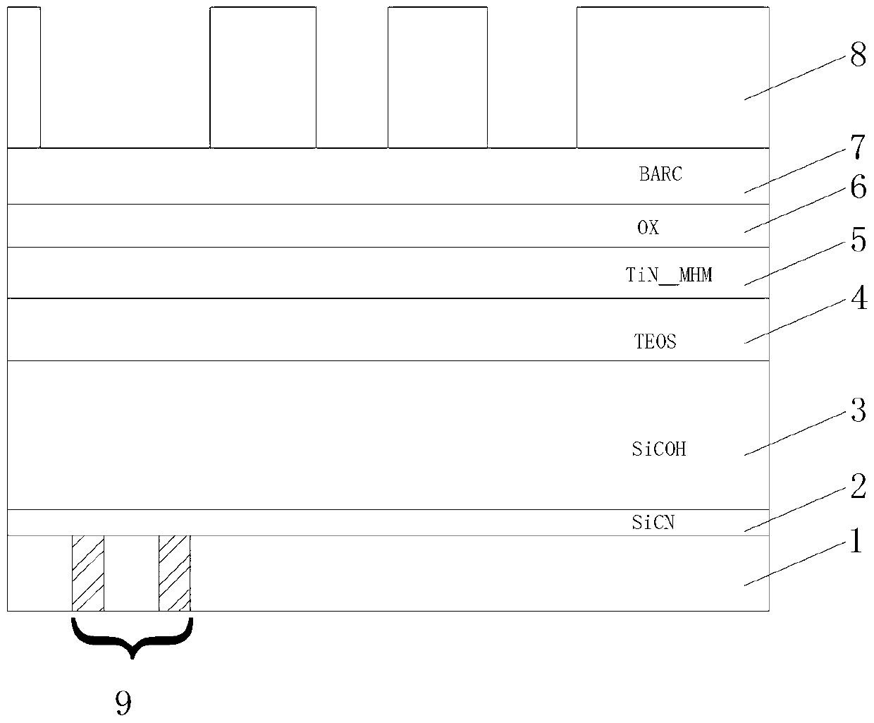
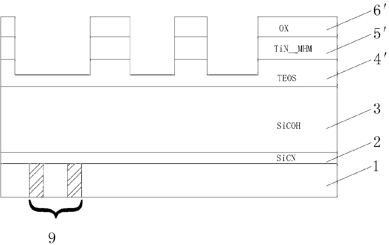
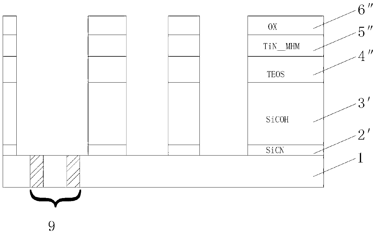
[0036] Step S1. Provide a semiconductor structure. The semiconductor structure includes a substrate 1. A dielectric layer, a metal hard mask 5 (TiN_MHM) and an oxide layer 6 (OX) are sequentially formed on the substrate 1 from bottom to top. The layers include the first dielectric layer 2 (SiCN), the second dielectric layer 3 (SiCOH), and the third dielectric layer 4 (TEOS) from bottom to top; there is a metal via region 9 in the substrate 1, and the metal via region 9 Partially filled with tungsten. In the copper interconnect trench etching process, it is necessary to o...


PUM


Abstract

The invention relates to the field of integrated circuit manufacturing, in particular to a method for decreasing the critical size of a copper-connection groove. In the manufacturing process of a mask of the copper-connection groove, after a traditional process is used for etching to a dielectric layer to form a first groove, a polymer layer is deposited on the surface of a device by the adoption of a plasma deposition process, the first groove is filled with the polymer layer, then plasma etching is conducted, the polymer layer is partially removed, the polymer layer with a certain thickness is reserved on the inner wall of the first groove, so that a second groove which is smaller in size compared with the critical size of an original pattern is formed, afterwards, the second groove is used for etching until a metal through hole area inside a substrate is exposed out of the substrate, and finally the polymer layer left in the groove is removed through the way of wet process cleaning so that the subsequent processes can be continued. According to the technical scheme, in the preparation technology of the copper-connection groove, the critical size of the groove can be decreased, the device performance can be enhanced, meanwhile production cost is low, and therefore the method for decreasing the critical size of the copper-connection groove is suitable for application and popularization.

Description

Technical field [0001] The invention relates to the field of integrated circuit manufacturing, in particular to a method for reducing the key dimensions of copper interconnect trenches. Background technique [0002] With the continuous development of technology, the critical size of semiconductor devices is getting smaller and smaller. The smaller the critical size of the device means the improvement of device performance. Those skilled in the art have been working hard to study which process to use to reduce the critical size of the device, and then Improve device performance. [0003] Figure 1-3 It is a flow chart of the manufacturing process of the key dimensions of copper interconnect trenches in the field of microelectronics in the prior art, which generally includes three steps: photolithography, metal hard mask etching, and metal trench etching: Step a: Provide a semiconductor Structure, the semiconductor structure includes a substrate 1, the substrate 1 is sequentially for...

Claims


Application Information

Patent Timeline
IPC IPC(8): H01L21/768
Inventor 韩冬曾林华任昱吕煜坤张旭昇
Owner SHANGHAI HUALI MICROELECTRONICS CORP
Why Eureka
Try Eureka