Responsivity-enhanced ZnO-based photoconductive detector and preparation method thereof

A photoconductive and enhanced technology, applied in the direction of semiconductor devices, circuits, electrical components, etc., can solve the problems of weak ultraviolet signal and low photoresponsivity, and achieve the effect of simple manufacturing process and improved photoresponsivity

Active Publication Date: 2013-10-09
徐州国隆电力配件铸造有限公司
View PDF3 Cites 20 Cited by
  • Summary
  • Abstract
  • Description
  • Claims
  • Application Information

AI Technical Summary

Problems solved by technology

[0003] However, on the road to practical application, the photoconductive wide bandgap semiconductor ultraviolet detector still has the disadvantage of low photoresponsivity, because in most applications, the ultraviolet signal to be detected is mostly very weak, which means The detector is required to have a high light detection rate

Method used


Image

  • Responsivity-enhanced ZnO-based photoconductive detector and preparation method thereof
  • Responsivity-enhanced ZnO-based photoconductive detector and preparation method thereof
  • Responsivity-enhanced ZnO-based photoconductive detector and preparation method thereof

Examples


preparation example Construction

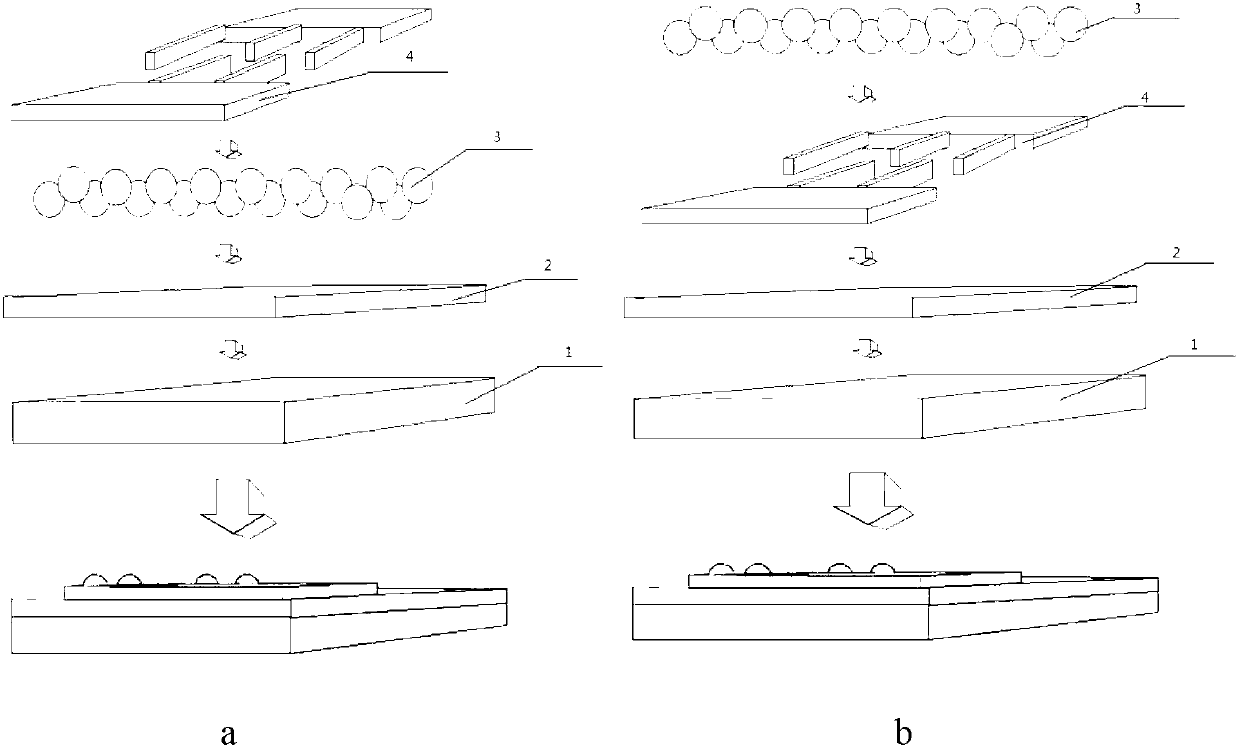
[0031] see figure 1 a, the method for preparing the response-enhanced ZnO-based photoconductive detector of the first structure of the present invention comprises the following steps:

[0032] 1) Clean the substrate 1, put it into the magnetron sputtering system, and evacuate the vacuum chamber to 8×10 -4 Below Pa, heat the substrate 1 to 200-400°C at the same time, and then feed argon and oxygen at the same time, so that the pressure of the vacuum chamber is 0.8-1.2Pa; then start to grow the ZnO thin film as the active layer with ZnO as the target material 2; Wherein, the volume flow ratio of argon gas and oxygen gas introduced is 25sccm: 35sccm, and the sputtering power is 70W when growing the ZnO thin film 2, and the time is 1.5 hours;

[0033] 2) Disperse Ag nanoparticles with a diameter of 50-150nm in deionized water to obtain an Ag nanoparticle dispersion; apply the Ag nanoparticle dispersion on the surface of the ZnO thin film 2 grown in step 1) with a spin coater, and...

Embodiment 1

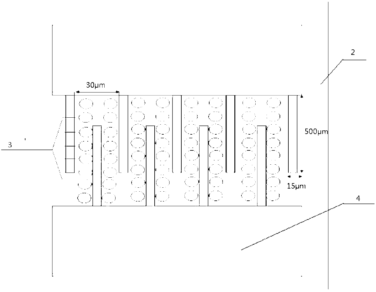
[0046] see figure 1 a, the first structure of the response-enhanced ZnO-based photoconductive detector of the present invention includes a quartz substrate and a ZnO film 2 disposed on the quartz substrate, and the ZnO film 2 is spin-coated with Ag nanoparticles 3, and the Ag nanoparticles Interdigitated Al electrodes 4 are also deposited on the interdigitated Al electrodes 4 , and part of the Ag nanoparticles 3 are exposed between adjacent fingers of the interdigitated Al electrodes 4 .

[0047] Among them, the thickness of the ZnO thin film 2 is 400nm; the diameter of the Ag nanoparticles is 100nm; the Ag nanoparticles 3 are spherical; The length is 500 μm and the interdigital width is 15 μm.

[0048] The preparation method of the response-enhanced ZnO-based photoconductive detector of this embodiment includes the following steps:

[0049] 1) Clean the quartz substrate, put it into the magnetron sputtering system, and evacuate the vacuum chamber to 5×10 -4 Pa, at the same...

Embodiment 2

[0055] see figure 1 b, the response-enhanced ZnO-based photoconductive detector of the present invention includes a quartz substrate and a ZnO thin film 2 disposed on the quartz substrate. An interdigitated Al electrode 4 is deposited on the ZnO thin film 2. On the interdigitated Al electrode 4 Ag nanoparticles 3 are filled between adjacent fingers, and the Ag nanoparticles 3 are spin-coated on the ZnO thin film 2 .

[0056] Among them, the thickness of the ZnO thin film 2 is 400nm; the Ag nanoparticles 3 are spherical; the height of the interdigitated Al electrode 4 is 150nm, the distance between adjacent interdigital fingers of the interdigitated Al electrode is 20 μm, the length of the interdigitated Al electrodes is 500 μm, and the width of the interdigitated Al electrodes is 500 μm. is 10 μm.

[0057] The preparation method of the response-enhanced ZnO-based photoconductive detector of this embodiment includes the following steps:

[0058] 1) Clean the quartz substrate,...


PUM

PropertyMeasurementUnit
thicknessaaaaaaaaaa
heightaaaaaaaaaa
diameteraaaaaaaaaa

Abstract

Disclosed are a responsivity-enhanced ZnO-based photoconductive detector and a preparation method thereof. The responsivity-enhanced ZnO-based photoconductive detector comprises a substrate and a ZnO film on the substrate. The ZnO film is coated with Ag nano-particles, fork-finger-shaped Al electrodes are deposited on the Ag nano-particles, and the Ag nano-particles are exposed among adjacent fork fingers of the fork-finger-shaped Al electrodes; or the fork-finger-shaped Al electrodes are deposited on the ZnO film, the Ag nano-particles are filled among the adjacent fork fingers of the fork-finger-shaped Al electrodes, and the Ag nano-particles are arranged on the ZnO film through spin-coating. The method includes the steps that the ZnO film is formed on the substrate through RF magnetron sputtering, then the Ag nano-particles are arranged on the ZnO film through spin-coating, or the fork-finger-shaped Al electrodes are deposited on the ZnO film; the responsivity-enhanced ZnO-based photoconductive detector can be obtained by depositing the fork-finger-shaped Al electrodes on the Ag nano-particles or arranging the Ag nano-particles on a sample surface with the fork-finger-shaped Al electrodes through spin-coating. According to the responsivity-enhanced ZnO-based photoconductive detector and the preparation method thereof, the surface plasma resonance effect of the Ag nano-particles is used for improving light absorbing ability of the detector, and therefore responsivity of the obtained photoconductive detector in an ultraviolet light area can be greatly improved.

Description

technical field [0001] The invention belongs to the field of wide-bandgap semiconductor ultraviolet detectors, and in particular relates to a response-enhanced ZnO-based photoconductive detector and a preparation method thereof. Background technique [0002] Ultraviolet detection materials and devices are a research direction that is developing rapidly in the field of optoelectronics. At present, the practical ultraviolet detectors are still mainly based on the first-generation photomultiplier tube and the second-generation silicon-based ultraviolet photodiode, but the former needs to be driven by high voltage, and has low efficiency, high cost, fragile and bulky. Bulky; the latter requires expensive filtering components, which have certain limitations for practical applications. In the past two decades, the third-generation wide-bandgap semiconductor technology represented by GaN, SiC and ZnO has developed rapidly, and a new generation of all-solid-state ultraviolet detect...

Claims


Application Information

Patent Timeline
Patent Type & Authority Applications(China)
IPC IPC(8): H01L31/0224H01L31/18
CPCY02P70/50
Inventor 张景文宋继东李高明李群孟鹂侯洵
Owner 徐州国隆电力配件铸造有限公司
Why Eureka
Try Eureka