Friction-nanogenerator-based molecular sensor
A technology of molecular sensors and nanogenerators, which is applied in the field of molecular sensors, can solve problems such as achievement reports, and achieve the effects of convenient production, convenient controllability, and small size
- Summary
- Abstract
- Description
- Claims
- Application Information
AI Technical Summary
Problems solved by technology
Method used
Image
Examples
Embodiment 1
[0098] Embodiment 1 Mercury ion sensor
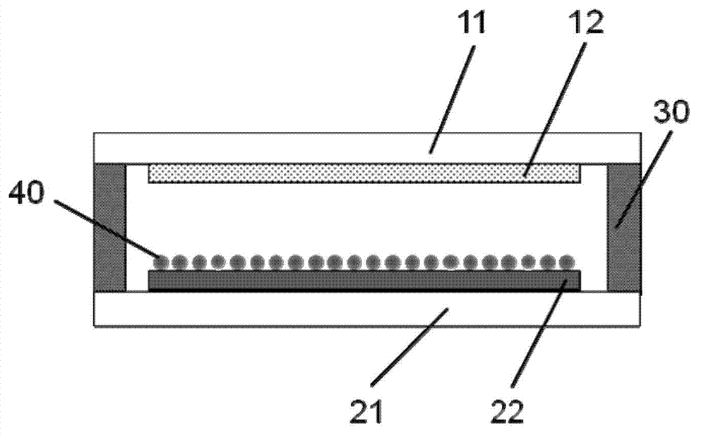
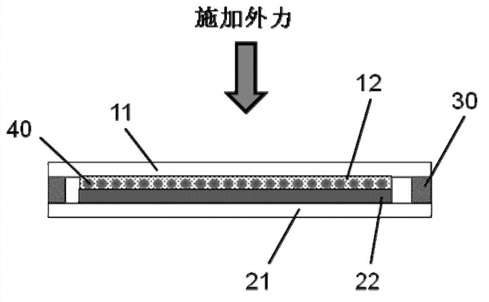
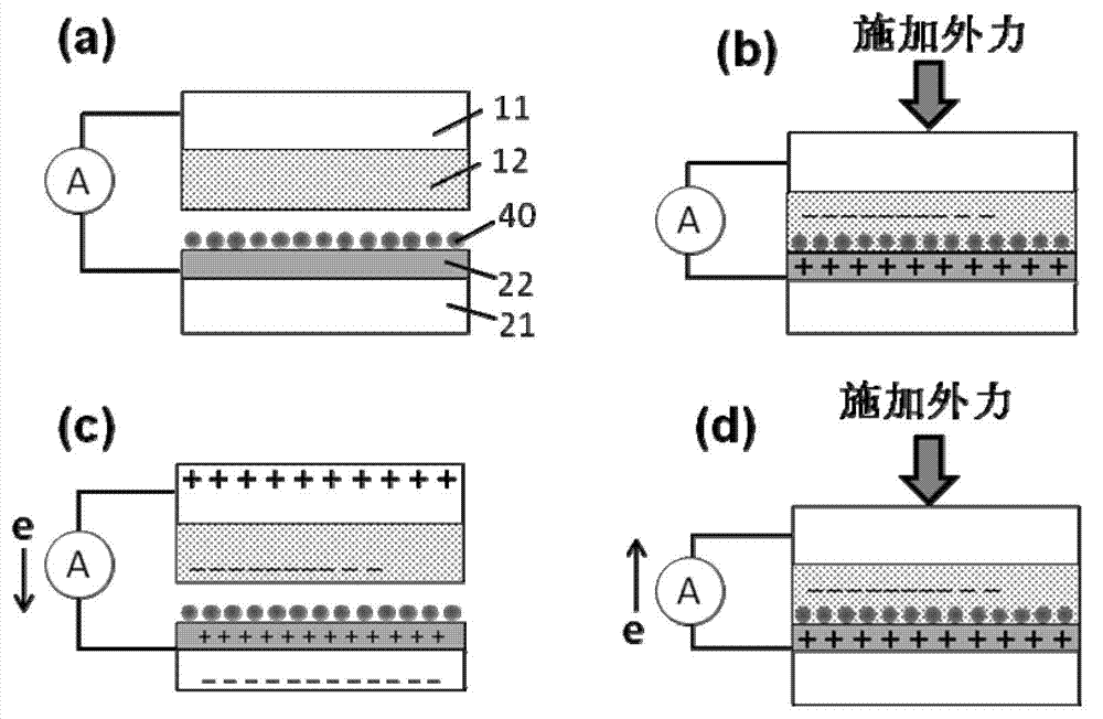
[0099] A metal gold film layer with a thickness of 50nm and a size of 1cm×1cm is used as the first conductive element, a polydimethylsiloxane (PDMS for short) film layer with a thickness of 10μm is used as the first friction layer, and a thickness of 50nm, A metal gold thin film layer with a size of 1cm×1cm is used as the second friction layer and the second conductive element, and then 1,3-dimercaptopropane (1,3-dimercaptopropane) is used to assemble gold nanoparticles with a size of 56nm, and then on the gold 3-Mercaptopropanoic acid (3-MPA) is modified on the nanoparticles to form a modified layer to achieve anti-mercury ion (Hg 2+ ) selectivity, which in turn becomes a mercury ion sensor, such as Figure 7 as shown in a.
[0100] Both the first insulating support layer and the second insulating support layer are plexiglass plates, and the two are connected by springs. For the connection method, see Figure 6 . When no external f...
Embodiment 2
[0103] Embodiment 2 lead ion sensor
[0104] A metal aluminum sheet with a thickness of 5mm and a size of 1cm×1cm is used as the first conductive element, and a polydimethylsiloxane (PDMS for short) film layer with a thickness of 40μm is used as the first friction layer. A metal copper thin plate of 1cm×1cm is used as the second conductive element, and a 100μm thick silicon wafer is used as the second friction layer, and a layer of photoresist is spin-coated, and a photoresist is formed on the photoresist by photolithography. Micron or sub-micron square window array; the second friction layer after photolithography is chemically etched with hot potassium hydroxide to form a pyramid-shaped concave structure array at the window. Then, polyacrylic acid molecules with specific adsorption to lead ions are supported on it to form a modification layer. Use elastic rubber as an insulating elastic connector to connect the metal copper sheet and the metal aluminum sheet, so that the PD...
Embodiment 3
[0105] Example 3 Escherichia coli sensor
[0106] The polyethylene sheet is used as two insulating supports, elastic glue is used as an insulating elastic connector, a thin layer of metallic silver with a thickness of 1 μm is used as the first conductive element, a polytetrafluoroethylene film with a thickness of 50 μm is used as the first friction layer, and a metal layer with a thickness of 1 μm is used as the first friction layer. Aluminum is used as the second friction layer and the second conductive layer, and nano-silver particles are loaded on its surface by vapor deposition, and thiolated mannose molecules are attached to form a modified layer to achieve highly selective adsorption of Escherichia coli. Among them, after depositing gold with a thickness of about 10 nanometers on the surface of the polytetrafluoroethylene film with a sputtering device, put it into an inductively coupled plasma etching machine, etch the side where the gold is deposited, and pass O 2 , Ar ...
PUM
| Property | Measurement | Unit |
|---|---|---|
| Thickness | aaaaa | aaaaa |
| Thickness | aaaaa | aaaaa |
Abstract
Description
Claims
Application Information


