Integrated broadband antenna and manufacturing method thereof

A production method and wide-band technology, applied in the directions of antenna grounding device, antenna support/mounting device, radiation element structure, etc., can solve problems such as increased antenna loss, impedance mismatch, and reduced bandwidth, and achieve reduced transmission distance, improve reliability, and reduce loss

Inactive Publication Date: 2015-02-18
SHANGHAI INST OF MICROSYSTEM & INFORMATION TECH CHINESE ACAD OF SCI
View PDF4 Cites 2 Cited by
  • Summary
  • Abstract
  • Description
  • Claims
  • Application Information

AI Technical Summary

Problems solved by technology

Although this method has many of the above advantages, the dielectric constant, thickness of the substrate material, and the size consistency of the antenna are poor, especially in relatively high frequency bands, and these errors will have a great impact on the antenna parameters. After it comes out, it needs further debugging before it can be used, which reduces the production efficiency and increases the cost
In addition, the traditional patch antenna and integrated circuit are separated, and when they are connected together, they will be limited by the connector, which will cause some problems: such as impedance matching, parasitic inductance, parasitic capacitance, etc.
However, this kind of antenna has a disadvantage, that is, the substrate is relatively thin, generally only tens of μm or even less than 1 μm, which greatly reduces the bandwidth.
It is difficult to increase the thickness of the substrate on silicon. The commonly used method in literature reports is to etch grooves on silicon, fill the grooves with solid dielectric materials to make the height consistent with the surroundings, and then use colloidal dielectric layers to make antenna patterns on top of them. In fact, this method makes the antenna substrate have at least two kinds of materials, the antenna loss increases, and the antenna pattern and the substrate material of the feeder are different, which is easy to cause impedance mismatch, and the simulation and process production are more troublesome; the other is in the slot Filling with the same dielectric material (usually liquid) as other areas, and then curing, this method can still be used when the depth of the groove is relatively shallow, but when the depth is large, it often leads to poor flatness of the antenna surface, adverse effect on the antenna

Method used


Image

  • Integrated broadband antenna and manufacturing method thereof
  • Integrated broadband antenna and manufacturing method thereof
  • Integrated broadband antenna and manufacturing method thereof

Examples


Embodiment 1

[0051] see Figure 1 to Figure 11 , as shown in the figure, the present invention provides a method for manufacturing an integrated broadband antenna, which at least includes the following steps:

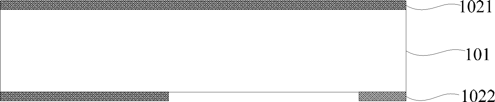
[0052] Such as figure 1 As shown, step 1) is first carried out, providing a Si substrate 101, and forming upper SiO on the upper and lower surfaces of the Si substrate. 2 Layer 1021 and lower SiO 2 layer 1022, under the SiO 2 A window is etched in layer 1022;

[0053] In this embodiment, the Si substrate 101 is oxidized by a thermal oxidation method to obtain the upper SiO 2 Layer 1021 and lower SiO 2 layer 1022, the upper SiO 2 Layer 1021 and lower SiO 2 Layers 1022 each have a thickness of 2 μm. Using BOE wet etch under the SiO 2 A window is etched in layer 1022 .

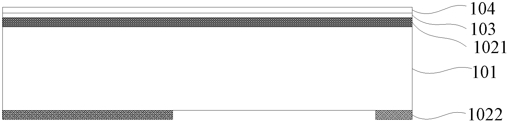
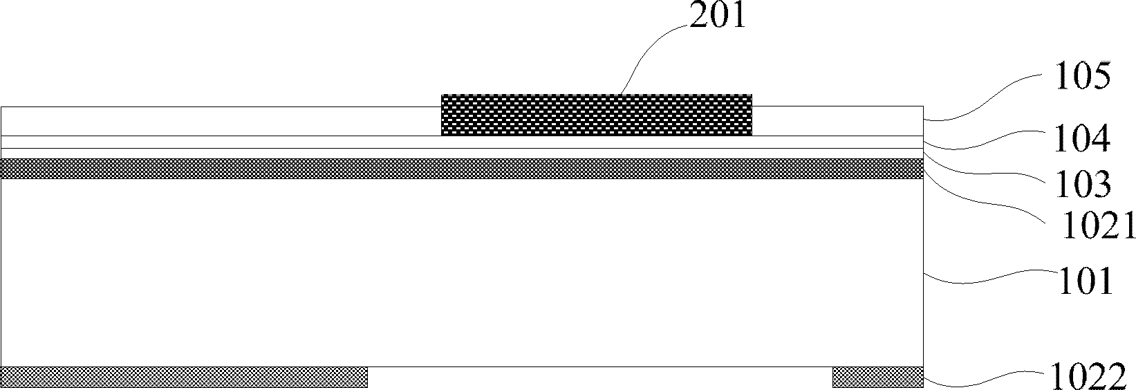
[0054] Such as Figure 2 ~ Figure 5b shown, and then proceed to step 2), on the SiO 2 Form the first seed layers 103-104 on the layer 1021, form a photoresist 201 on the first seed layer corresponding to th...

Embodiment 2

[0063] see Figure 10a ~ Figure 10c , the present invention also provides an integrated broadband antenna, at least including: a support structure, the support structure has a dielectric cavity 115; The region has a groove structure 106; solder balls 107, welded to the ground plane and used as the lead-out end of the ground plane; an organic dielectric layer 108, covering the ground plane and the groove structure 106; pattern antenna 111 ˜113 includes an antenna main body located in a vertical area on the dielectric cavity 115 and combined with the organic dielectric layer 108 and a feeder extending from the antenna main body toward the solder ball 107 . It should be noted that the shape of the pattern antennas 111 - 113 may be rectangular, circular, elliptical, polygonal, clothoid, or other desired shapes. Since the dielectric constant of the dielectric cavity 115 is the dielectric constant of vacuum or air, and the value is about 1, the dielectric substrate of the antenna c...


PUM


Abstract

The invention provides an integrated broadband antenna and a manufacturing method thereof. A grounding surface is manufactured on a Si substrate, and an organic dielectric material with fluidity is manufactured on the grounding surface and is solidified to be a substrate of the antenna. An antenna pattern is manufactured on the substrate, and the Si substrate of a corresponding region of the antenna pattern is etched so that a medium cavity is formed. A defect that a silicon-based antenna medium substrate is relatively thin is conquered by the integrated broadband antenna. Compared with a conventional silicon-based integrated antenna, the bandwidth of the antenna is significantly enhanced and the performance of the antenna is enhanced. The manufacturing technology process of the integrated broadband antenna is compatible to an embedded type chip packaging so that the manufactured antenna can be packaged together with the chip. Compared with an external connecting method of the antenna, a transmission distance of a signal line is reduced so that the loss is reduced. Meanwhile, the antenna is integrated with the chip so that the reliability is enhanced, the size is reduced and the trend of modern integrated circuit packaging is met.

Description

technical field [0001] The invention relates to an antenna and a manufacturing method thereof, in particular to an integrated broadband antenna and a manufacturing method thereof. Background technique [0002] In the field of wireless communication, antenna is an indispensable and very important part. The microstrip antenna is a new type of antenna successfully developed in the early 1970s. Compared with commonly used microwave antennas, it has the following advantages: small size, light weight, low profile, conformal to the carrier, simple manufacture, and low cost; the characteristic of electrical appliances is that it can obtain a single-directional wide-lobe pattern, The maximum radiation direction is in the normal direction of the plane, easy to integrate with microstrip lines, and easy to realize linear polarization or circular polarization. Microstrip antennas with the same structure can form a microstrip antenna array to obtain higher gain and larger bandwidth. Th...

Claims


Application Information

Patent Timeline
Patent Type & Authority Patents(China)
IPC IPC(8): H01Q1/22H01Q1/38H01Q1/48
Inventor 王天喜罗乐徐高卫
Owner SHANGHAI INST OF MICROSYSTEM & INFORMATION TECH CHINESE ACAD OF SCI
Why Eureka
Try Eureka