Method for preparing orderly gallium nitride nano pillar array with ultraviolet soft imprinting

A gallium nitride nanometer and soft embossing technology, which is applied in the direction of nanotechnology, optomechanical equipment, photoplate making process of pattern surface, etc., can solve the problems that there are no nanostructure light-emitting diodes, etc., to improve light extraction efficiency and improve Internal Quantum Efficiency, Effect of Internal Quantum Efficiency Improvement

Active Publication Date: 2013-11-06
NANJING UNIV
View PDF4 Cites 34 Cited by
  • Summary
  • Abstract
  • Description
  • Claims
  • Application Information

AI Technical Summary

Problems solved by technology

From the currently disclosed UV soft imprinting technology (see Chinese patents CN201110148202.7, CN201110087571.X), there is no use of PMMA and UV-curable adhesive double-layer adhesive structure to prepare nitride nano-arrays
And this preparation of nanostructures can be used to pattern gallium nitride substrates (see Chinese patent CN201010617750.5), and use photolithography, nanoimprinting technology, etc. to pattern the light-emitting diodes or introduce photonic crystals to improve the light output of light

Method used


Image

  • Method for preparing orderly gallium nitride nano pillar array with ultraviolet soft imprinting
  • Method for preparing orderly gallium nitride nano pillar array with ultraviolet soft imprinting
  • Method for preparing orderly gallium nitride nano pillar array with ultraviolet soft imprinting

Examples


Embodiment Construction

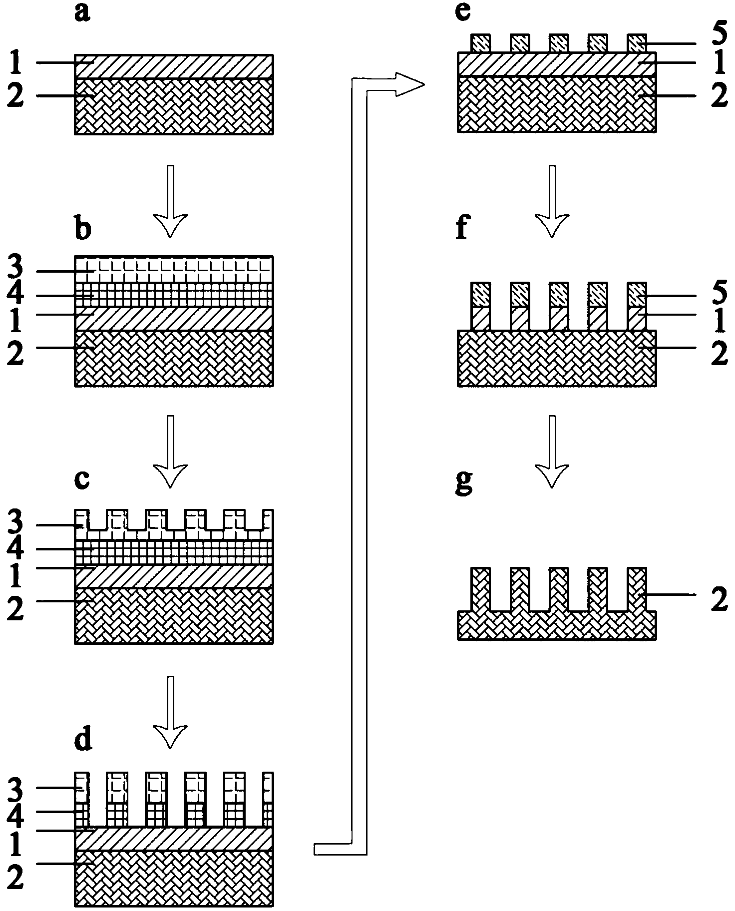
[0032] The present invention prepares a large-area and low-defect gallium nitride nanocolumn (hole) array through an ultraviolet soft imprinting technique, and uses reactive ion etching to control the diameter of the nanocolumn (hole) in the dielectric layer, thereby Realize controllable diameter of gallium nitride nanopillars (holes).

[0033] figure 1 Among them, 1 represents silicon dioxide or silicon nitride, 2 represents gallium nitride substrate, 3 represents UV curing adhesive, 4 represents PMMA, and 5 represents metal nickel or chromium. figure 1 a-1f represents each technological process. Figure 5 11 represents gallium nitride, 12 represents n-type gallium nitride, 13 represents indium gallium nitrogen quantum well, and 14 represents p-type gallium nitride. The luminous intensity of the gallium nitride nanocolumn (hole) array is greatly improved, especially the internal quantum efficiency is improved, and it is suitable for preparing a nanocolumn (hole) type light ...


PUM

PropertyMeasurementUnit
Thicknessaaaaaaaaaa
Thicknessaaaaaaaaaa
Thicknessaaaaaaaaaa

Abstract

Provided is a method for preparing an orderly gallium nitride nano pillar array with ultraviolet soft imprinting. A dielectric film is grown on a gallium nitride substrate, a metal orderly nano pillar (hole) structure is obtained through an ultraviolet soft imprinting double-layer stripping technology, a dielectric film nano pillar (hole) structure with a changeable and adjustable diameter is obtained through a reactive ion etching method, and inductively coupled plasma is used for being etched to obtain the gallium nitride orderly nano pillar (hole) array with different diameters. The dielectric film which comprises SiO2 and SiNx is grown on the gallium nitride substrate, and PMMA and ultraviolet curing glue coat the surface of a substrate sample in a rotary mode in sequence. A large-area low-defect orderly nano hole (pillar) array structure is formed on the ultraviolet curing glue through an ultraviolet soft imprinting technology, residual glue and the PMMA are then etched through a reactive ion etching technology, and the metal nano pillar (hole) array structure is obtained by stripping an evaporated metallic film. A dielectric film layer structure is etched through the reactive ion etching method, and the dielectric nano pillar (hole) structure with the changeable and adjustable diameter is obtained.

Description

technical field [0001] The invention relates to a preparation method of a gallium nitride-based III nitride ordered nanocolumn (hole) array, in particular to the realization of a large-area and low-defect nanocolumn (hole) array structure using ultraviolet soft imprinting technology, and The method of using reactive ion etching to control the diameter of nanocolumns (holes) on the basis of ensuring the original periodic structure makes up for the singleness of nanostructures prepared by nanoimprinting technology, and involves nanocolumns InGaN-GaN The invention relates to a preparation method of a quantum well, which belongs to the fields of nanometer material science and technology and low-dimensional photoelectric devices. Background technique [0002] Group III nitride materials are direct bandgap semiconductors, and their bandgap covers from infrared to visible light to ultraviolet bands. They are ideal materials for solid-state lighting and low-power displays. Solid-st...

Claims


Application Information

Patent Timeline
IPC IPC(8): H01L33/00G03F7/00B82Y40/00
Inventor 刘斌张荣庄喆葛海雄郭旭谢自力陈鹏修向前赵红陈敦军陆海顾书林韩平郑有炓
Owner NANJING UNIV
Why Eureka
Try Eureka