Method and device for growing bismuth selenide single crystal film on silicon substrate

A bismuth selenide single crystal and silicon substrate technology, applied in ion implantation plating, coating, electrical components, etc., can solve the problems of high cost and high lattice mismatch, and achieve the effect of low cost and simple operation

Inactive Publication Date: 2013-11-20
UNIV OF ELECTRONICS SCI & TECH OF CHINA
View PDF6 Cites 13 Cited by
  • Summary
  • Abstract
  • Description
  • Claims
  • Application Information

AI Technical Summary

Problems solved by technology

[0010] In order to overcome the technical defects of high lattice mismatch and high cost in the prior art, the present invention discloses a method and device for growing a bismuth selenide single crystal film on a silicon substrate

Method used


Image

  • Method and device for growing bismuth selenide single crystal film on silicon substrate
  • Method and device for growing bismuth selenide single crystal film on silicon substrate
  • Method and device for growing bismuth selenide single crystal film on silicon substrate

Examples


Embodiment 1

[0050] Example 1.Bi 2 Se 3 Growth of Single Crystal Thick Film

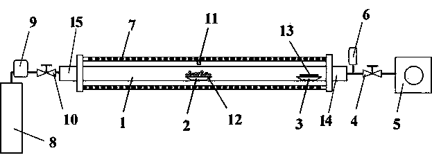
[0051] in such as figure 1 The specific steps for growing a bismuth selenide single crystal thin film on a silicon substrate with a thickness exceeding 200nm are as follows:

[0052] The highly pure (99.999%) compound microchip Bi 2 Se 3 The evaporation source 12 is placed in the quartz crucible 2 located in the center of the quartz tube 1 in the vacuum tube furnace body, and the area after cleaning and passivation process is 1×1 cm 2 The (111) oriented silicon substrate 13 is placed on the movable quartz sample holder 3 near the first nozzle 14, and the quartz sample holder 3 is moved so that the distance between the center of the Si substrate 13 and the right port of the quartz tube 1 is 15 cm.

[0053] After sealing the quartz tube 1, open the stop valve 4, and use the vacuum pump 5 located at one end of the vacuum tube furnace to evacuate the quartz tube 1 to a vacuum. Observe the vacuum gauge 6. When...

Embodiment 2

[0064] Example 2 Bi 2 Se 3 Growth of Single Crystal Ultrathin Films

[0065] in such as figure 1 The specific steps for growing a bismuth selenide single crystal thin film on a silicon substrate with a thickness of 20nm are as follows:

[0066] High-purity (99.99%) compound powder Bi 2 Se 3 The evaporation source 12 is placed in the quartz crucible 2 located in the center of the quartz tube 1 in the vacuum tube furnace body, and the area after the chemical cleaning and passivation process is 0.5 × 1cm 2 The (111) oriented silicon substrate 13 is placed on the movable quartz sample holder 3, the long side of the silicon substrate is adjusted to be perpendicular to the axial direction of the quartz tube, and the quartz sample holder 3 is moved so that the center of the silicon substrate 13 is at a distance from the quartz tube. 1 The distance between the ports on the right side is 12cm.

[0067] After the quartz tube 1 is sealed, the stop valve 4 is opened, and the quar...


PUM

PropertyMeasurementUnit
thicknessaaaaaaaaaa

Abstract

The invention relates to a method for growing a bismuth selenide single crystal film on a silicon substrate. The method comprises the following steps: 1, chemically cleaning the surface of single crystal silicon and performing etching passivation to obtain the silicon substrate; 2, placing Bi2Se3 compound and the silicon substrate at a tubular furnace quartz tube center region and a first tube opening, sealing a quartz tube and vacuumizing; 3, heating the quartz tube center region; 4, introducing inert carrier gas from a second tube opening of the quartz tube to begin to grow a film; and 5, after film growth is completed, stop introducing argon and heating, introducing shielding gas to fill in the quartz tube after the temperature of the quartz tube is cooled, and then taking out a sample. The invention also relates to a device for growing the bismuth selenide single crystal film on the silicon substrate. According to the method and the device for growing the bismuth selenide single crystal film on the silicon substrate, the Bi2Se3 single crystal film is prepared on the common Si silicon substrate with a physical vapor transportation deposition device, the operation is simple, the cost is low, and the epitaxial single crystal film with high quality can be prepared.

Description

technical field [0001] The invention belongs to the field of semiconductor materials, and relates to a method and a device for growing a bismuth selenide single crystal thin film on a silicon substrate. Background technique [0002] Bi 2 Se 3 It is a newly revealed class of strong topological insulator materials (topological insulator is a kind of internal insulation, and the interface allows charge to move). Up to 0.3 electron volts, far exceeding the thermal oscillator energy at room temperature. A single Dirac cone surface energy band makes Bi 2 Se 3 It has become the most ideal system to study the quantum phenomena related to Dirac fermions, and at the same time, the larger bulk energy bandgap makes Bi 2 Se 3 It has the potential to be applied at room temperature. Therefore Bi 2 Se 3 It is one of the topological insulator materials with the most scientific research value and practical application potential discovered so far. As far as scientific research and de...

Claims


Application Information

Patent Timeline
Patent Type & Authority Applications(China)
IPC IPC(8): H01L21/31C23C14/06C23C14/54
Inventor 李含东高磊李辉王高云罗思源任武洋艾远飞巫江周志华王志明
Owner UNIV OF ELECTRONICS SCI & TECH OF CHINA
Why Eureka
Try Eureka