Groove gate VDMOS device integrated with Schottky diode

A Schottky diode and Schottky junction technology, applied in the direction of diodes, semiconductor devices, electrical components, etc., can solve the problems of VDMOS device switching characteristics deterioration, high stored charge diode peak reverse current, device dynamic failure, etc.

Inactive Publication Date: 2013-12-11
UNIV OF ELECTRONIC SCI & TECH OF CHINA +1
View PDF5 Cites 26 Cited by
  • Summary
  • Abstract
  • Description
  • Claims
  • Application Information

AI Technical Summary

Problems solved by technology

The reverse recovery of the body diode has a greater impact on the switching process of the VDMOS device, especially during the turn-on process of the VDMOS device, the reverse recovery process of the body diode may cause overshoot of current and voltage, resulting in dynamic failure of the device, and wors

Method used


Image

  • Groove gate VDMOS device integrated with Schottky diode
  • Groove gate VDMOS device integrated with Schottky diode
  • Groove gate VDMOS device integrated with Schottky diode

Examples


Embodiment 1

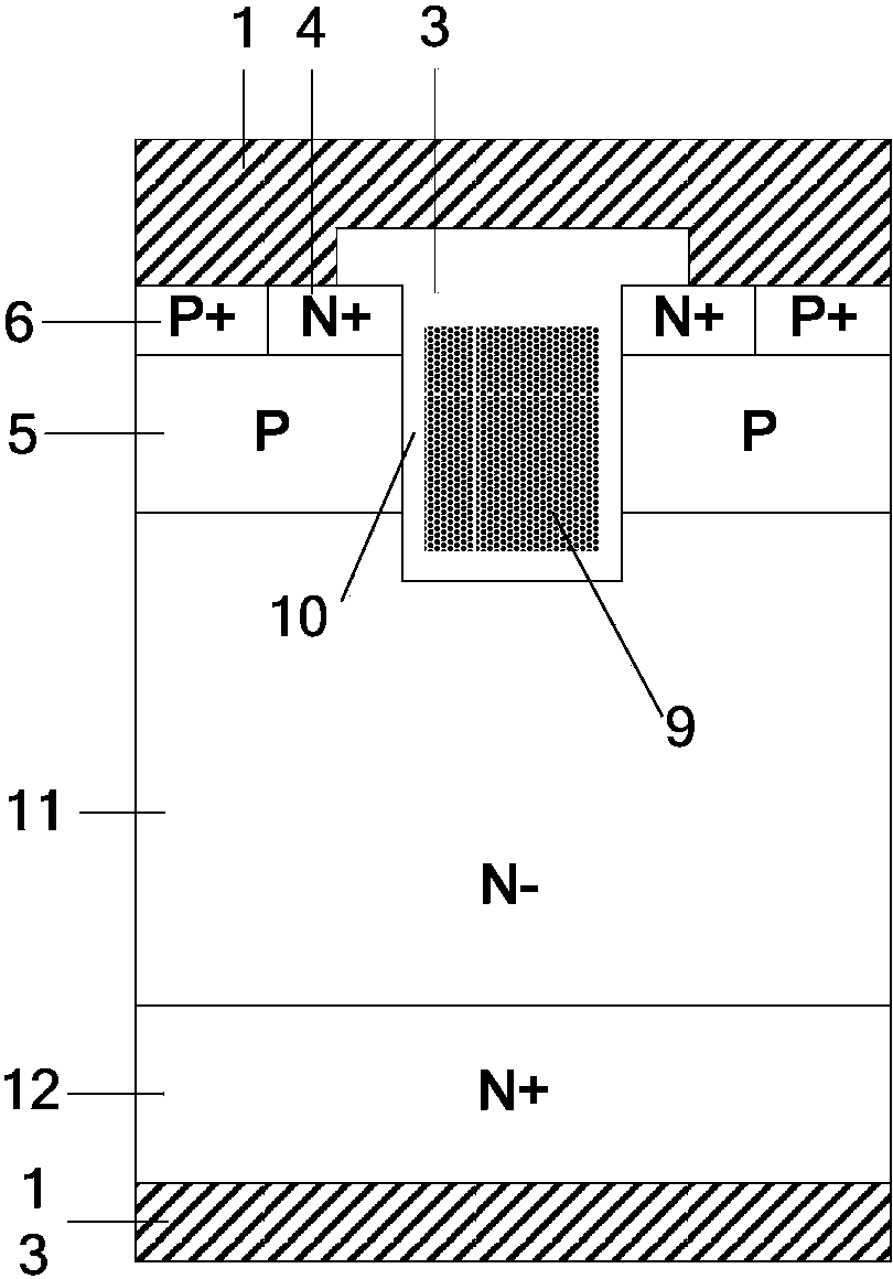
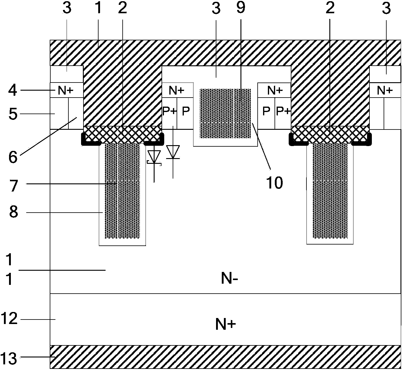
[0032] figure 2 It shows a specific embodiment of the groove gate VDMOS device integrating Schottky diodes proposed by the present invention, including: a highly doped semiconductor substrate 12 of the first conductivity type, and a back contact with the semiconductor substrate 12 of the highly doped first conductivity type The drain metal 13 and the low-doped first-conductivity-type semiconductor drift region 11 in front contact with the highly-doped first-conductivity-type semiconductor substrate 12; A second conductivity type semiconductor body region 5, in each second conductivity type semiconductor body region 5 has a highly doped first conductivity type semiconductor source region 4 and a highly doped second conductivity type semiconductor body contact region 6 which are independent of each other , the surfaces of the highly doped first conductivity type semiconductor source region 4 and the highly doped second conductivity type semiconductor body contact region 6 are i...

Embodiment 2

[0047] Such as Figure 6.1 As shown, compared with Embodiment 1, the process of Embodiment 2 is generally the same, except that a second layer of low-doped first-conductivity-type semiconductor is added to the surface of the low-doped first-conductivity-type semiconductor drift region 11 (first epitaxial layer). Epitaxial layer 15.

[0048] According to needs, the turn-on voltage and withstand voltage of the Schottky diode can be adjusted by adjusting the concentration of the second epitaxial layer 15, and adjusting the concentration will also slightly affect the forward conduction characteristics of the device, reducing the doping of the second epitaxial layer 15 Concentration can increase the withstand voltage of the Schottky junction, but at the same time it will increase the resistance of the drift region, so that the conduction voltage drop will increase slightly, and a compromise design can be made according to the specific situation.

Embodiment 3

[0050] Such as Figure 6.2 As shown, compared with Embodiment 1, the polysilicon gate electrode 10 and the polysilicon body electrodes 7 on both sides adopt the same groove depth in Embodiment 3.

[0051] Using the same trench depth, the gate electrode trench and the body electrode trenches on both sides can be formed in the same etching process, which can reduce the etching process steps; in addition, this design can optimize the forward resistance more effectively. The electric field distribution in the off-time drift region is because mutual protection can be formed between the grooves from the top of the groove to the bottom where the electric field lines are densest, and the locally concentrated electric field lines are dispersed, and the withstand voltage of the device can be further improved.


PUM


Abstract

The invention discloses a groove gate VDMOS device integrated with a Schottky diode and belongs to the technical field of semiconductor devices. According to the groove gate VDMOS device integrated with the Schottky diode, an additional structure composed of a piece of Schottky junction metal and a body electrode conductive material is additionally arranged on each of drift regions on the two sides of a groove gate structure of a conventional groove gate VDMOS device, the upper portion of each piece of Schottky junction metal is in contact with source electrode metal, the lower portion of each piece of Schottky junction metal is in contact with a corresponding body electrode conductive material, and the lower surface and the lateral sides of the each piece Schottky junction metal are in contact with a corresponding drift region to form a Schottky junction; dielectric layers are arranged between the lateral sides of each body electrode conductive material and a corresponding drift region and between the bottom surface of each body electrode conductive material and the corresponding drift region. Compared with a traditional groove gate VDMOS device with the same size, the groove gate VDMOS device integrated with the Schottky diode has the advantages that due to the fact that higher drift region dosage concentration is adopted under the condition of same puncture voltage, turn-on resistance is reduced obviously, and the reverse recovery property of the diode is improved obviously.

Description

technical field [0001] The invention belongs to the technical field of semiconductor devices, and relates to a trench gate VDMOS device, in particular to a trench gate VDMOS device integrated with a Schottky diode. Background technique [0002] VDMOS is the most widely used type of power device in power semiconductors. It has the advantages of easy driving, fast switching speed, integration, and simple process. In the low-voltage field, the trench-gate VDMOS device is widely used because it eliminates the resistance of the JFET region and has a smaller cell size, so it has a lower specific on-resistance. [0003] The basic N-channel trench-gate VDMOS device structure is as figure 1 As shown, it includes: source metal 1, isolation dielectric 3, N+ source region 4, P-type base region 5, P+ body contact region 6, polysilicon gate electrode 9, gate dielectric layer 10, N-drift region 11, N+ liner bottom 12 and drain metal 13. VDMOS devices are often used as switching devices....

Claims


Application Information

Patent Timeline
IPC IPC(8): H01L29/78H01L29/06H01L29/872H01L29/40
CPCH01L29/7813H01L29/407H01L29/41766H01L29/42368H01L29/7806
Inventor 任敏宋洵奕吴明进杨文韬单亚东顾鸿鸣宋文龙李泽宏张金平张波
Owner UNIV OF ELECTRONIC SCI & TECH OF CHINA
Why Eureka
Try Eureka