Hydride vapor deposition device and method for improving thickness distribution uniformity of multiple-piece epitaxial materials
A hydride gas phase and thickness distribution technology, which is applied in the manufacture of electrical components, discharge tubes, semiconductors/solid-state devices, etc., can solve problems such as the inability to meet the requirement that the thickness uniformity of the chip is less than ±5%, and achieve improved utilization and High production efficiency, strong economical practicability, and high utilization
- Summary
- Abstract
- Description
- Claims
- Application Information
AI Technical Summary
Problems solved by technology
Method used
Image

Examples
Embodiment 1
[0060] The technical scheme of embodiment one:
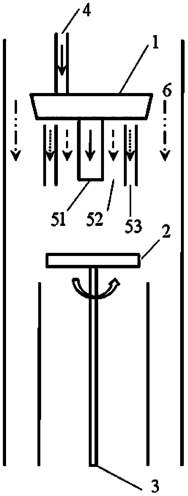
[0061] 1. Surface pretreatment of sapphire substrate: Place a commercially purchased sapphire substrate that can be directly epitaxy in MOCVD equipment, and pass it into a protective atmosphere, including but not limited to nitrogen, ammonia, inert gas, hydrogen and other gases, at a temperature of 1000 ~1200℃, keep warm for 10~120 minutes;
[0062] 2. Preparation of MOCVD template: After the surface of the sapphire substrate is pretreated, the temperature is lowered to 550-600° C., and a low-temperature buffer layer is grown with a thickness of 30-60 nm. The low-temperature buffer layer is conducive to releasing the stress generated by the epitaxy of the heterogeneous substrate. Then raise the temperature to 900-1100°C to grow a high-temperature GaN / sapphire composite substrate with a GaN thickness of 3-6 μm;
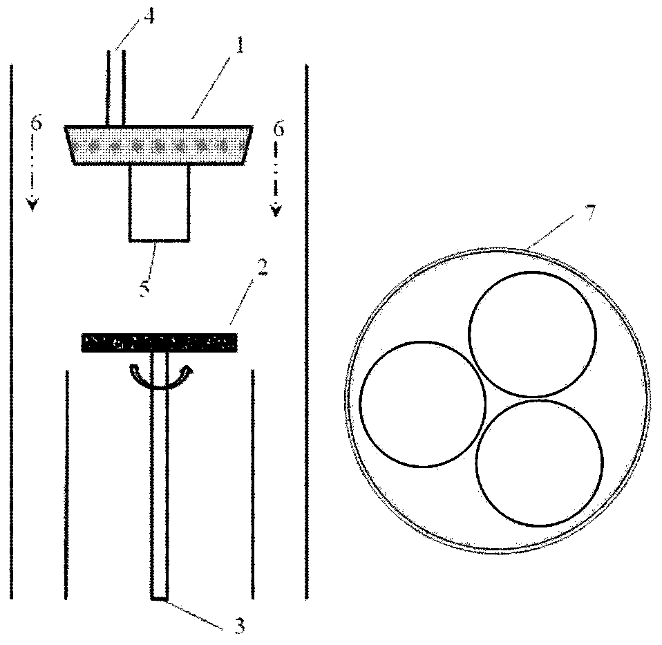
[0063] 3. HVPE secondary epitaxial high-quality thin film: 3 pieces of MOCVD-grown GaN / sapphire templates are attach...
Embodiment 2
[0064] The technical scheme of embodiment two:
[0065] 1. Surface pretreatment of sapphire substrate: Place a commercially purchased sapphire substrate that can be directly epitaxy in MOCVD equipment, and pass it into a protective atmosphere, including but not limited to oxygen, nitrogen, ammonia, inert gas, hydrogen and other gases, Temperature 1000~1200℃, keep warm for 10~120 minutes;
[0066] 2. Preparation of MOCVD template: After the surface of the sapphire substrate is pretreated, the temperature is lowered to 550-600° C., and a low-temperature buffer layer is grown with a thickness of 30-60 nm. The low-temperature buffer layer is conducive to releasing the stress generated by the epitaxy of the heterogeneous substrate. Then raise the temperature to 900-1100°C to grow high-temperature GaN / sapphire template, the thickness of GaN is 3-6μm;
[0067] 3. HVPE secondary epitaxial high-quality thin film: 7 GaN / sapphire templates grown by MOCVD are attached Figure 6 The pos...
Embodiment 3
[0068] The technical scheme of embodiment three:
[0069] 1. Surface pretreatment of sapphire substrate: Place a commercially purchased sapphire substrate that can be directly epitaxy in MOCVD equipment, and pass it into a protective atmosphere, including but not limited to oxygen, nitrogen, ammonia, inert gas, hydrogen and hydrogen chloride, etc. Gas, temperature 1000~1200℃, keep warm for 10~120 minutes;
[0070] 2. Preparation of MOCVD template: After the surface of the sapphire substrate is pretreated, the temperature is lowered to 550-600° C., and a low-temperature buffer layer is grown with a thickness of 30-60 nm. The low-temperature buffer layer is conducive to releasing the stress generated by the epitaxy of the heterogeneous substrate. Then raise the temperature to 900-1100°C to grow high-temperature GaN / sapphire template, the thickness of GaN is 3-6μm;
[0071] 3. HVPE secondary epitaxial high-quality thin film: 19 GaN / sapphire templates grown by MOCVD are attached...
PUM
| Property | Measurement | Unit |
|---|---|---|
| Thickness | aaaaa | aaaaa |
| Thickness | aaaaa | aaaaa |
| Thickness | aaaaa | aaaaa |
Abstract
Description
Claims
Application Information
 - R&D
- Intellectual Property
- Life Sciences
- Materials
- Tech Scout
- Unparalleled Data Quality
- Higher Quality Content
- 60% Fewer Hallucinations
Browse by: Latest US Patents, China's latest patents, Technical Efficacy Thesaurus, Application Domain, Technology Topic, Popular Technical Reports.
© 2025 PatSnap. All rights reserved.Legal|Privacy policy|Modern Slavery Act Transparency Statement|Sitemap|About US| Contact US: help@patsnap.com