Preparation method of nanopore chip with plasmon resonance scattering response function

A plasmon resonance and nanopore technology, applied in the direction of material excitation analysis, etc., to achieve the effect of simple steps, low cost, and controllable size

Inactive Publication Date: 2014-01-15
EAST CHINA UNIV OF SCI & TECH
View PDF3 Cites 7 Cited by
  • Summary
  • Abstract
  • Description
  • Claims
  • Application Information

AI Technical Summary

Problems solved by technology

However, what it obtains is only the static information of the molecules to be measured on the surface of the noble metal

Method used


Image

  • Preparation method of nanopore chip with plasmon resonance scattering response function
  • Preparation method of nanopore chip with plasmon resonance scattering response function
  • Preparation method of nanopore chip with plasmon resonance scattering response function

Examples


Embodiment 1

[0030] A method for preparing a nanopore chip with plasmon resonance scattering response, the steps comprising:

[0031] (1) Selection of chip substrate

[0032] Choose Thick 100 A silicon wafer is used as a chip substrate, and an insulating material with a thickness of 5 nm is deposited on the front side of the silicon wafer, and the insulating material is silicon nitride; there is no insulating material on the reverse side of the silicon wafer.

[0033] (2) Fabrication of chips

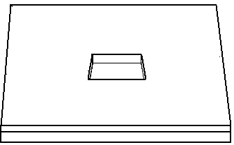
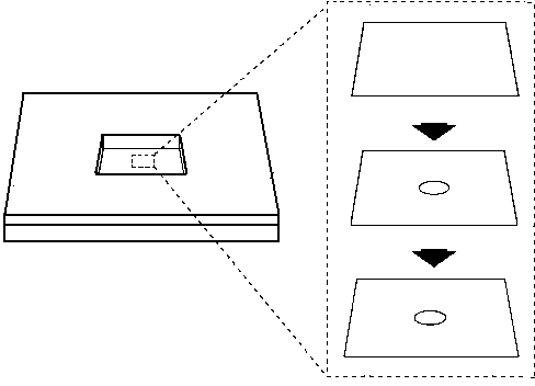
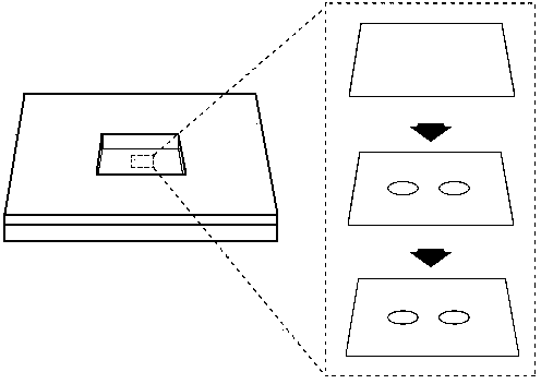
[0034] Etch a side length of 100mm on the reverse side of the silicon wafer in step (1) by wet etching The square area is etched until the insulating material silicon nitride is exposed; the etched square area is the nanoporous chip film (see figure 1 ).

[0035] (3) Nanopore etching

[0036] Place the chip described in step (2) in a plasma cleaner for 5 minutes to wash away the pollutants in the film of the nanoporous chip; then place the chip backside up in a vacuum chamber, when the vacuum...

Embodiment 2

[0040] A method for preparing a nanopore chip with plasmon resonance scattering response, the steps comprising:

[0041] (1) Selection of chip substrate

[0042] Choose Thick 300 A silicon wafer is used as the chip substrate, and an insulating material with a thickness of 50 nm is deposited on the front side of the silicon wafer, and the insulating material is aluminum oxide; there is no insulating material on the reverse side of the silicon wafer.

[0043] (2) Fabrication of chips

[0044] Use wet etching to etch a side length of 300mm on the reverse side of the silicon wafer in step (1). The square area is etched until the insulating material alumina is exposed; the etched square area is the nanoporous chip film (see figure 1 ).

[0045] (3) Nanopore etching

[0046] Place the chip described in step (2) in a plasma cleaner for 5 minutes to wash away the pollutants in the film of the nanoporous chip; then place the chip backside up in a vacuum chamber, when the vacuum ...

Embodiment 3

[0050] A method for preparing a nanopore chip with plasmon resonance scattering response, the steps comprising:

[0051] (1) Selection of chip substrate

[0052] Choose Thick 500 A silicon wafer is used as the chip substrate, and an insulating material with a thickness of 100 nm is deposited on the front side of the silicon wafer, and the insulating material is silicon dioxide; there is no insulating material on the reverse side of the silicon wafer.

[0053] (2) Fabrication of chips

[0054] Use wet etching to etch a side length of 500mm on the back side of the silicon wafer in step (1). The square area is etched until the insulating material silicon dioxide is exposed; the etched square area is the nanoporous chip film (see figure 1 ).

[0055] (3) Nanopore etching

[0056] Place the chip described in step (2) in a plasma cleaner for 5 minutes to wash away the pollutants in the film of the nanoporous chip; then place the chip backside up in a vacuum chamber, when the ...


PUM

PropertyMeasurementUnit
pore sizeaaaaaaaaaa

Abstract

The invention discloses a preparation method of a nanopore chip with a plasmon resonance scattering response function. The preparation method comprises the following steps: (1) selecting a chip substrate: selecting a silicon chip as a substrate, and depositing an insulating material on the front surface of the silicon chip, without the insulating material on the back surface; (2) etching a square area on the back surface of the silicon chip by a wet etching method until a nanopore chip film is exposed on the back surface; (3) etching nanopores: forming the nanopores on the nanopore chip film by using a focused ion beam or a focused electron beam to bomb the nanopore chip film; (4) modifying noble metal: coating a noble metal layer on the surface of the nanopore chip film by using a magnetron sputtering instrument. The preparation method is simple in steps; the prepared nanopore chip is controllable in size and relatively low in cost; through noble metal modification on the nanopores, the nanopore chip with a photoelectric response function is prepared; the nanopore chip can cause a plasmon resonance coupling phenomenon so as to amplify a spectral signal, and can be applied to many fields such as electrochemical detection of the nanopores.

Description

technical field [0001] The invention relates to the technical fields of nanopore electrical analysis and detection technology and nanometer scattering spectrum analysis, in particular to a method for preparing a nanopore chip with plasma resonance scattering response. Background technique [0002] Nanopore electrochemical detection technology is a technology that uses the detection of the weak ion current characteristic electrical signal generated when a single molecule passes through a nanometer-sized channel driven by an electric field to study the individual behavior of biomolecules. Because the physical occupation of a single molecule to be tested in the nanopore changes the conductance of the hole, the ion current flowing through the nanopore changes, forming a blocking current signal. The current intensity, blocking time and signal shape of each blocking current signal are directly related to the individual behavior information of the single molecule in the nanopore. ...

Claims


Application Information

Patent Timeline
Patent Type & Authority Applications(China)
IPC IPC(8): G01N21/63
Inventor 龙亿涛顾震李萌应佚伦周浩
Owner EAST CHINA UNIV OF SCI & TECH
Why Eureka
Try Eureka