Oxide thin film transistor and manufacturing method thereof
A technology of oxide thin film and manufacturing method, which is applied in the direction of transistor, semiconductor/solid-state device manufacturing, semiconductor device, etc., and can solve the problem of unstable performance of IGZO thin film transistor
- Summary
- Abstract
- Description
- Claims
- Application Information
AI Technical Summary
Problems solved by technology
Method used
Image
Examples
Embodiment 1
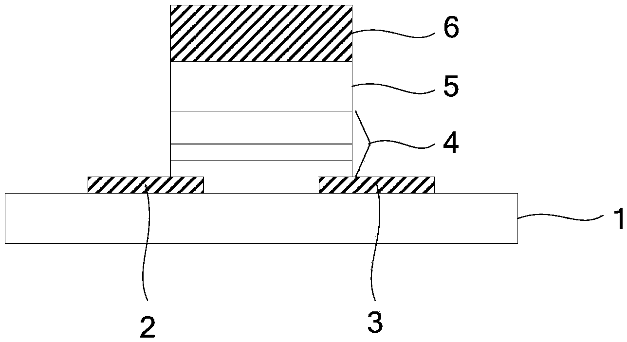
[0032] The stacked oxide semiconductor layer in this embodiment is composed of an IGZO thin film layer (1:1:1:4) and a spacer layer. The spacer layer is an alloy of Hf and Nd, where the atomic number ratio of Nd:Hf is 2%. The spacer layer target and the IGZO (1:1:1:4) target were installed at two different target positions, and the spacer layer and the IGZO thin film layer were stacked by radio frequency sputtering.
[0033] Argon is used as the sputtering gas, the sputtering pressure is between 0.1Pa-10.0Pa, the substrate temperature is maintained at room temperature to 150°C during sample growth, the sputtering power is 40-200W, and the background vacuum of the sputtering chamber is less than 1× 10 -7 Torr, the total thickness of the prepared stacked oxide semiconductor film is 50nm, and the order of sputtering coating is the first IGZO thin film layer (20nm), the hafnium neodymium alloy thin film layer (10nm) and the second IGZO thin film layer (20nm). Anneal in air for 3...
Embodiment 2
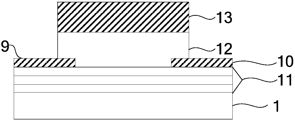
[0046] The stacked oxide semiconductor in this embodiment is composed of IGZO (1:1:1:4) and spacer layers therebetween. The spacer layer is an alloy of hafnium oxide and neodymium oxide, where the atomic number ratio of Nd:Hf is 5%. The spacer layer target and the IGZO (1:1:1:4) target were installed on two different target positions, and the spacer layer and the IGZO layer were stacked by radio frequency sputtering.
[0047] Argon is used as the sputtering gas, the sputtering pressure is between 0.1Pa-10.0Pa, the substrate temperature is maintained at room temperature to 150°C during sample growth, the sputtering power is 40-200W, and the background vacuum of the sputtering chamber is less than 1× 10 -7 Torr, the total thickness of the prepared stacked oxide semiconductor film is 60nm, and the sputtering coating sequence is the first IGZO thin film layer (25nm), the hafnium neodymium alloy thin film layer (10nm) and the second IGZO thin film layer (25nm). The stacked films ...
Embodiment 3
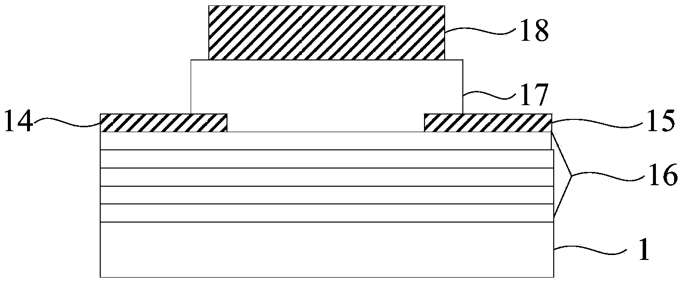
[0057] The stacked oxide semiconductor in this embodiment is composed of IGZO thin film layers (1:1:1:4) and spacer layers between the thin film layers. The spacer layer is an alloy of hafnium oxide and neodymium oxide, where the atomic number ratio of Nd:Hf is 1%. The spacer layer target and the IGZO (1:1:1:4) target were installed on two different target positions, and the spacer layer and the IGZO layer were stacked by radio frequency sputtering.
[0058] Argon is used as the sputtering gas, the sputtering pressure is between 0.1Pa-10.0Pa, the substrate temperature is maintained at room temperature to 150°C during sample growth, the sputtering power is 40-200W, and the background vacuum of the sputtering chamber is less than 1× 10 -7 The total thickness of the prepared stacked oxide semiconductor film is 40nm, and the sputtering coating sequence is the first IGZO thin film layer (10nm), the first hafnium neodymium alloy thin film layer (5nm), and the second IGZO thin film ...
PUM
| Property | Measurement | Unit |
|---|---|---|
| thickness | aaaaa | aaaaa |
| thickness | aaaaa | aaaaa |
| thickness | aaaaa | aaaaa |
Abstract
Description
Claims
Application Information


