Flexible organic light emitting diode and method for manufacturing same

A luminescent and diode technology, applied in the field of organic electroluminescent devices, can solve the problems affecting the luminous stability of OLED devices, weak bonding force of flexible substrates, and high surface resistance of conductive films, so as to be easy to popularize and use, and enhance luminous stability Good performance and stability

Inactive Publication Date: 2014-01-29
OCEANS KING LIGHTING SCI&TECH CO LTD +1
View PDF0 Cites 2 Cited by
  • Summary
  • Abstract
  • Description
  • Claims
  • Application Information

AI Technical Summary

Problems solved by technology

However, these conductive films also have many insurmountable problems in the application of flexible OLEDs.
For example, low-temperature sputtering technology is usually used to prepare conductive films such as ITO on flexible substrates. The prepared conductive films not only have high surface resistance, but also have weak bonding force with flexible substrates, so that flexible OLEDs can withstand repeated bending. During the process, the conductive film is prone to fall off from the flexible substrate, which affects the light emission stability of the OLED device

Method used


Image

  • Flexible organic light emitting diode and method for manufacturing same
  • Flexible organic light emitting diode and method for manufacturing same
  • Flexible organic light emitting diode and method for manufacturing same

Examples


Embodiment 1

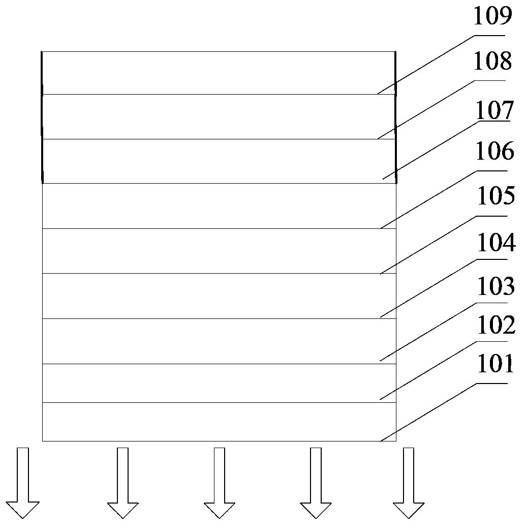
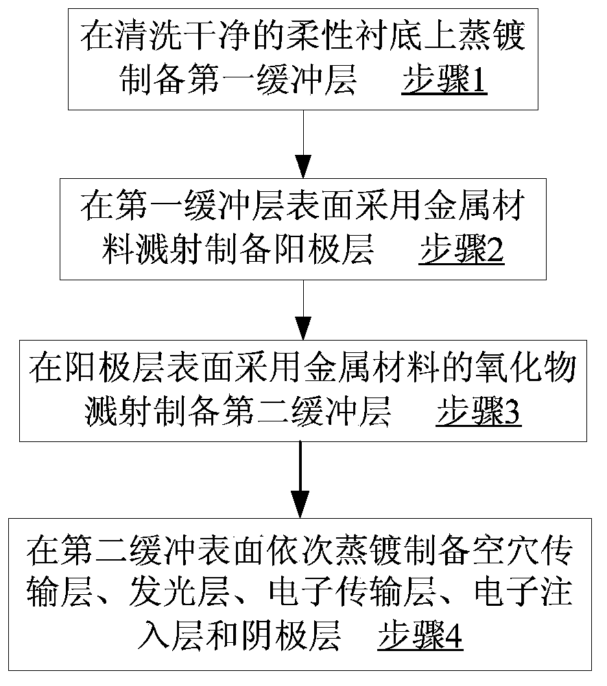
[0039] A flexible OLED with a layered structure ( Figure 1a ), consisting of sequentially stacked flexible substrate 101, first buffer layer 102, anode layer 103, second buffer layer 104, hole transport layer 105, light emitting layer 106, electron transport layer 107, electron injection layer 108 and cathode layer 109 Composition, wherein the flexible substrate 101 is PEN, the first buffer layer 102 is 200nm SiO, the anode layer 103 is 18nm Al, the second buffer layer is 1nm aluminum oxide, and the hole transport layer 105 is 40nm NPB , the light-emitting layer 106 is 25nm TCTA: Ir(ppy) 3 Doped structure (TCTA: Ir(ppy) 3 =100:3, where, TCTA:Ir(ppy) 3 It is expressed as a doped mixed material, and the description below is similar), the electron transport layer 107 is 35nm TPBi, the electron injection layer is 1nm LiF, and the cathode layer 108 is 70nm Al. The flexible OLED is a bottom emitting device. The manufacturing method of the light emitting device comprises the foll...

Embodiment 2

[0046] A flexible OLED with a layered structure, consisting of a flexible substrate, a first buffer layer, an anode layer, a second buffer layer, a hole transport layer, a light emitting layer, an electron transport layer, an electron injection layer and a cathode layer stacked in sequence, Among them, the flexible substrate is PET, the first buffer layer is 200nm ZrO 2 , the anode layer is 20nm Ag, the second buffer layer is 2nm silver oxide, the hole transport layer is 40nm NPB, and the light emitting layer is 25nm TCTA:Ir(ppy) 3 Doped structure (TCTA: Ir(ppy) 3 =100:3), the electron transport layer is 35nm TPBi, the electron injection layer is 1nm LiF, and the cathode layer is 30nm Sm. The flexible OLED is a double-sided light emitting device. Its manufacturing method is the same as that of Example 1, and will not be repeated here.

Embodiment 3

[0048] A flexible OLED with a layered structure, consisting of a flexible substrate, a first buffer layer, an anode layer, a second buffer layer, a hole transport layer, a light emitting layer, an electron transport layer, an electron injection layer and a cathode layer stacked in sequence, Among them, the flexible substrate is PES, the first buffer layer is 200nm TiO 2 , the anode layer is 70nm Ni, the second buffer layer is 5nm nickel oxide, the hole transport layer is 40nm NPB, and the light emitting layer is 25nm TCTA:Ir(ppy) 3 Doped structure (TCTA: Ir(ppy) 3 =100:3), the electron transport layer is 35nm TPBi, the electron injection layer is 1nm LiF, and the cathode layer is 30nm Yb. The flexible OLED is a top-emitting light-emitting device. Its manufacturing method is the same as that of Example 1, and will not be repeated here.


PUM


Abstract

The invention discloses a flexible organic light emitting diode and a method for manufacturing the same. The flexible organic light emitting diode comprises a flexible substrate, an anode layer, a second buffer layer, a hole transport layer, a light emitting layer, an electron transport layer, an electron injection layer and a cathode layer which are sequentially stacked on one another. The anode layer is made of metal materials, and a first buffer layer which is used for increasing binding force between the flexible substrate and the anode layer is further arranged between the flexible substrate and the anode layer and is made of silicon monoxide, zirconium dioxide or titanium dioxide. The flexible organic light emitting diode and the method have the advantages that the anode layer is made of the metal materials, so that surface resistance of the anode layer can be reduced; the first buffer layer is arranged between the anode layer and the flexible substrate and can increase the binding force between the flexible substrate and the anode layer, so that the anode layer can be prevented from dropping off from the flexible substrate, and the light emitting stability of the finally manufactured light emitting diode can be improved; a process for manufacturing the flexible organic light emitting diode is simple and is easy to implement.

Description

technical field [0001] The invention belongs to the technical field of organic electroluminescent devices, and relates to an organic electroluminescent diode and a manufacturing method thereof. More specifically, the present invention relates to a flexible organic electroluminescent diode and its manufacturing method. Background technique [0002] Organic electroluminescent diodes (referred to as OLEDs) have the characteristics of high brightness, wide range of material selection, low driving voltage, and full-cure active light emission. The development trend of the display, while meeting the requirements of green lighting technology, is the focus of many researchers at home and abroad. [0003] Among the OLED devices in the prior art, OLED devices made of glass substrates lack bending properties and are fragile, which limits the popularization and application of light emitting devices. OLED devices using flexible materials as substrates are lighter, thinner, and more impa...

Claims


Application Information

Patent Timeline
Patent Type & Authority Applications(China)
IPC IPC(8): H01L51/50H01L51/52
CPCH10K77/10H10K50/81H10K71/00Y02E10/549Y02P70/50
Inventor 周明杰王平冯小明陈吉星
Owner OCEANS KING LIGHTING SCI&TECH CO LTD
Why Eureka
Try Eureka