Marine microorganism adhesion sensor based on organic electrochemical transistor and preparation method of sensor
A technology of marine microorganisms and transistors, applied in the field of biosensors, can solve problems such as equipment stability and safety impact, loss of working ability, and microbial fouling of marine engineering equipment, achieving low cost, simple structure, and easy on-site long-term monitoring. Effect
- Summary
- Abstract
- Description
- Claims
- Application Information
AI Technical Summary
Problems solved by technology
Method used
Image
Examples
Embodiment 1
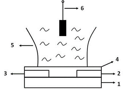
[0039] A marine microbial sensor based on an organic electrochemical transistor consists of a substrate 1, a drain electrode 2 and a source electrode 3, a conductive polymer layer 4, a water storage tank 5, and a gate electrode 6, and the drain electrode 2 and source electrode 3 are located between the substrate 1 Above, the conductive polymer layer 4 connects the drain electrode 2 and the source electrode 3, the water storage tank 5 is located on the conductive polymer layer 4, the gate electrode 6 is located in the water storage tank 5, suspended above the conductive polymer layer 4, through the electrolyte and The conductive polymer layer 4 is connected. The conductive polymer layer is made of conductive polymer poly(3,4-dioxyethylthiophene) / polystyrene sulfonic acid (PEDOT:PSS).
[0040] The glass substrate was cleaned by ultrasonic cleaning with deionized water, acetone and absolute ethanol for 10 min respectively. After cleaning, put the glass substrate into a UV surfac...
Embodiment 2
[0043] The PET polyester film was cleaned by ultrasonic cleaning with deionized water, acetone and absolute ethanol for 10 min respectively. After cleaning, put it into a UV surface irradiation cleaning machine for cleaning for 10 minutes; use a vacuum evaporation method to evaporate the source electrode and the drain electrode, the source and drain electrodes are Cu electrodes, the evaporation rate is 0.2 nanometers per second, and the thickness is 10 nanometers; Spin-coat the conductive polymer layer polypyrrole (PPy) at a speed of 2000 rpm with a thickness of 5nm; then anneal at 200°C for 1 hour under a nitrogen atmosphere; then fix the silicone tube on the surface of the device with glue and seal it into a water storage pool ; Finally, the silver / silver chloride electrode is inserted into the water storage tank as a grid; the organic electrochemical transistor marine microbial sensor is obtained.
Embodiment 3
[0045]The silicon wafer substrate was cleaned by ultrasonic cleaning with deionized water, acetone, and absolute ethanol for 10 min respectively. After cleaning, put it into a UV surface irradiation cleaning machine for cleaning for 10 minutes; use the vacuum evaporation method to evaporate the source electrode and the drain electrode, the source and drain electrodes are both indium tin oxide (ITO) electrodes, and the evaporation rate is 0.6 nm / s. The thickness is 300 nm; the conductive polymer layer polyaniline is spin-coated at a speed of 2000 rpm with a thickness of 80 nm; then annealed at 200 ° C for 1 hour in a nitrogen atmosphere; then the silicone tube is fixed on the surface of the device with glue and sealed into a A water storage tank; finally, a gold wire electrode is inserted into the water storage tank as a grid; an organic electrochemical transistor marine microbial sensor is obtained.
PUM
| Property | Measurement | Unit |
|---|---|---|
| Thickness | aaaaa | aaaaa |
| Thickness | aaaaa | aaaaa |
Abstract
Description
Claims
Application Information
 - R&D
- Intellectual Property
- Life Sciences
- Materials
- Tech Scout
- Unparalleled Data Quality
- Higher Quality Content
- 60% Fewer Hallucinations
Browse by: Latest US Patents, China's latest patents, Technical Efficacy Thesaurus, Application Domain, Technology Topic, Popular Technical Reports.
© 2025 PatSnap. All rights reserved.Legal|Privacy policy|Modern Slavery Act Transparency Statement|Sitemap|About US| Contact US: help@patsnap.com


