

Method for preparing ultra-thin copper seed crystal layer on diffusion barrier layer and application thereof
A technology of copper seed layer and barrier layer, which is applied in coating, metal material coating process, semiconductor/solid-state device manufacturing, etc., can solve problems such as difficult film uniformity, improve performance and reliability, increase precision Effect of ability to control, ability to improve
- Summary
- Abstract
- Description
- Claims
- Application Information
AI Technical Summary
Problems solved by technology
Method used
Image

Examples
Embodiment 1
[0041] The copper interconnect structure is prepared as follows:
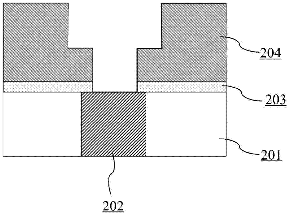
[0042] Step A. If figure 1As shown, on the substrates 201 and 202 after any layer of an interconnection structure is wired, an etch stop layer 203 is deposited first, and then an insulating dielectric layer 204 is deposited.
[0043] The material of the insulating dielectric layer 204 is silicon dioxide SiO 2 , the material of the etch stop layer 203 is silicon nitride.
[0044] Step B. If figure 1 As shown, the interconnected trenches are formed by photolithographic etching using a standard dual damascene process flow.
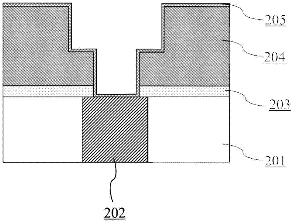
[0045] Step C. If figure 2 As shown, the Ta / TaN diffusion barrier layer 205 is deposited by magnetron sputtering.
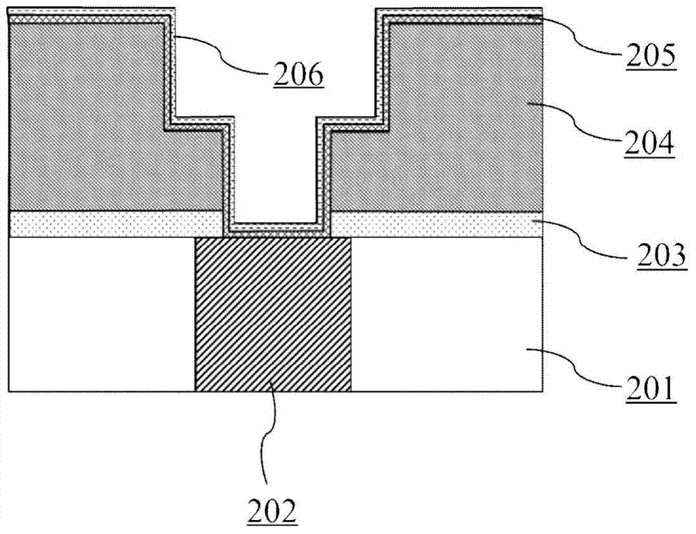
[0046] Step D. If image 3 As shown, an ultra-thin copper seed layer 206 is prepared on the barrier layer by atomic layer deposition.
[0047] The precursors for depositing the ultra-thin copper seed layer are bis(hexafluoroacetylacetonate) copper and diethyl zinc, and th...
Embodiment 2
[0056] The copper interconnect structure is prepared as follows:
[0057] Step A. If figure 1 As shown, on the substrates 201 and 202 after any layer of an interconnection structure is wired, an etch stop layer 203 is deposited first, and then an insulating dielectric layer 204 is deposited.
[0058] The material of the insulating dielectric layer 204 is silicon dioxide SiO 2 , the material of the etch stop layer 203 is silicon nitride.
[0059] Step B. If figure 1 As shown, the interconnected trenches are formed by photolithographic etching using a standard dual damascene process flow.
[0060] Step C. If figure 2 As shown, the Ta / TaN diffusion barrier layer 205 is deposited by magnetron sputtering.
[0061] Step D. If image 3 As shown, an ultra-thin copper seed layer 206 is prepared on the barrier layer by atomic layer deposition.
[0062] The precursors for depositing the ultra-thin copper seed layer are bis(hexafluoroacetylacetonate) copper and diethyl zinc, and t...
Embodiment 3
[0071] The copper interconnect structure is prepared as follows:
[0072] Step A. If figure 1 As shown, on the substrates 201 and 202 after any layer of an interconnection structure is wired, an etch stop layer 203 is deposited first, and then an insulating dielectric layer 204 is deposited.
[0073] The material of the insulating dielectric layer 201 is fluorinated silicon dioxide SiOF, and the material of the etching stop layer is silicon nitride.
[0074] Step B. If figure 1 As shown, photolithographic etching forms interconnected trenches 210 .
[0075] Step C. If figure 2 As shown, the Ta / TaN diffusion barrier layer 205 is deposited by magnetron sputtering.
[0076] Step D. If image 3 As shown, an ultra-thin copper seed layer 206 is prepared on the barrier layer by atomic layer deposition.
[0077] The precursors for depositing the ultra-thin copper seed layer are bis(hexafluoroacetylacetonate) copper and diethyl zinc, and the bis(hexafluoroacetylacetonate) copper...
PUM
 Abstract
Description
Claims
Application Information