Method and application for preparing ultra-thin copper seed layer by processing surfaces of hydrogen plasmas

A copper seed layer, hydrogen plasma technology, applied in semiconductor/solid-state device manufacturing, electrical components, circuits, etc., can solve the problems of poor adhesion, multi-impurities in thin films, etc., to increase adhesion, reduce impurity content, The effect of reducing contact resistance

Inactive Publication Date: 2014-03-26
FUDAN UNIV
View PDF3 Cites 4 Cited by
  • Summary
  • Abstract
  • Description
  • Claims
  • Application Information

AI Technical Summary

Problems solved by technology

However, since ALD is a surface chemical deposition technique, it is inevitable that the deposited film contains more impurities and poor adhesion

Method used


Image

  • Method and application for preparing ultra-thin copper seed layer by processing surfaces of hydrogen plasmas
  • Method and application for preparing ultra-thin copper seed layer by processing surfaces of hydrogen plasmas
  • Method and application for preparing ultra-thin copper seed layer by processing surfaces of hydrogen plasmas

Examples


Embodiment 1

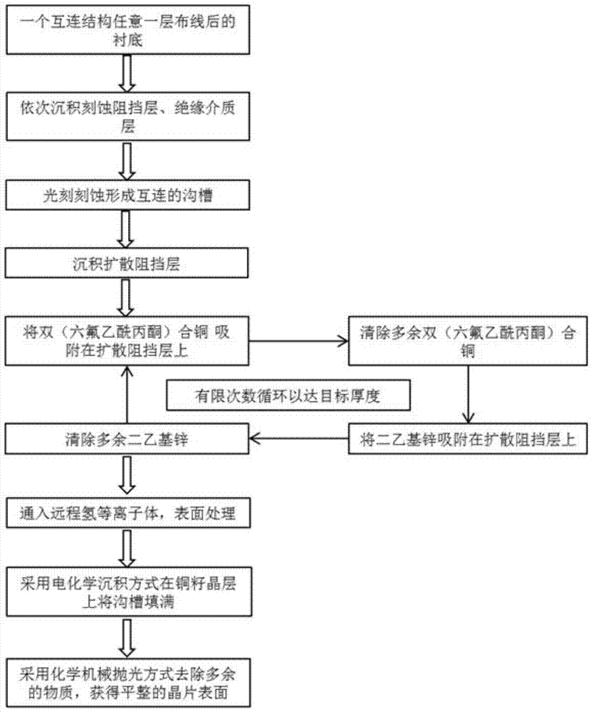
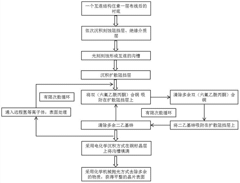
[0049] A remote hydrogen plasma surface treatment was performed after the ALD deposition of an ultra-thin copper seed layer.

[0050] The copper interconnect structure is prepared as follows:

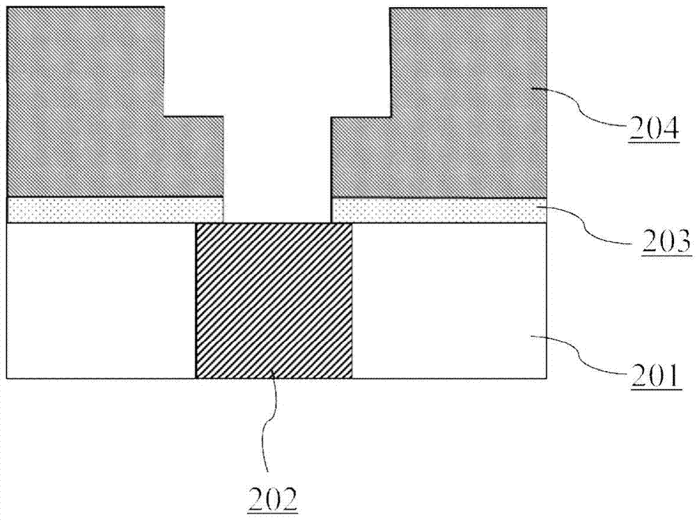
[0051] Step A. If image 3 As shown, on the substrates 201 and 202 after any layer of an interconnection structure is wired, an etch stop layer 203 is deposited first, and then an insulating dielectric layer 204 is deposited.

[0052] The material of the insulating dielectric layer 204 is silicon dioxide SiO 2 , the material of the etch stop layer 203 is silicon nitride.

[0053] Step B. If image 3 As shown, the interconnected trenches are formed by photolithographic etching using a standard dual damascene process flow.

[0054] Step C. If Figure 4 As shown, the Ta / TaN diffusion barrier layer 205 is deposited by magnetron sputtering.

[0055] Step D. If Figure 5 As shown, a high-quality ultra-thin copper seed layer 206 is prepared on the barrier layer, and the specific steps a...

Embodiment 2

[0069] Remote hydrogen plasma surface treatment during ALD deposition of ultrathin copper seed layers.

[0070] The copper interconnect structure is prepared as follows:

[0071] Step A. If image 3 As shown, on the substrates 201 and 202 after any layer of an interconnection structure is wired, an etch stop layer 203 is deposited first, and then an insulating dielectric layer 204 is deposited.

[0072] The material of the insulating dielectric layer 204 is fluorinated silicon dioxide SiOF, and the material of the etching stop layer 203 is silicon nitride.

[0073] Step B. If image 3 As shown, the interconnected trenches are formed by photolithographic etching using a standard dual damascene process flow.

[0074] Step C. If Figure 4 As shown, the Ta / TaN diffusion barrier layer 205 is deposited by magnetron sputtering or the like.

[0075] Step D. If Figure 5 As shown, an ultra-thin copper seed layer 206 is prepared on the barrier layer, and the specific steps are as ...

Embodiment 3

[0087] Remote hydrogen plasma surface treatment during ALD deposition of ultrathin copper seed layers.

[0088] The copper interconnect structure is prepared as follows:

[0089] Step A. If image 3 As shown, on the substrates 201 and 202 after any layer of an interconnection structure is wired, an etch stop layer 203 is deposited first, and then an insulating dielectric layer 204 is deposited.

[0090] The material of the insulating dielectric layer 201 is porous hydrocarbon-doped silicon oxide SiCO:H, and the material of the etching stopper layer is silicon nitride.

[0091] Step B. If image 3 As shown, photolithographic etching forms interconnected trenches 210 .

[0092] Step C. If Figure 4 As shown, the Ta / TaN diffusion barrier layer 205 is deposited by magnetron sputtering.

[0093] Step D. If Figure 5 As shown, an ultra-thin copper seed layer 206 is prepared on the barrier layer, and the specific steps are as follows.

[0094]The precursors for depositing the ...


PUM


Abstract

The invention belongs to the technical field of semiconductor integrated circuits, specifically a method for preparing an ultra-thin copper seed layer by processing surfaces of remote hydrogen plasmas. The method disclosed by the invention comprises the following steps: absorbing bi(hexafluoro-acetylacetone) copper on a diffusion barrier layer to remove residual bi(hexafluoro-acetylacetone) copper; absorbing diethyl zinc on the diffusion barrier layer to remove residual diethyl zinc; repeating the above steps to achieve the target thickness of the ultra-thin copper seed layer; finally inputting the remote hydrogen plasmas to process the surface. With an ALD (Atomic Layer Deposition) method, the copper seed layer is grown, the thickness of the copper seed layer can be effectively controlled under lower technique temperature, and the copper seed layer has good groove filling performance; with remote hydrogen plasmas pulse, gas byproducts can be generated by reacting with impurities in a deposition film and are taken away through carrier gas, thus the quality of the deposition film is improved, the adhesion characteristic of electro-coppering and the copper seed layer is improved, and the reliability in the copper-connection application of the integrated circuits is kept.

Description

technical field [0001] The invention belongs to the technical field of semiconductor integrated circuits, and in particular relates to a method for improving the quality of an atomic layer deposition ultra-thin copper seed layer by remote hydrogen plasma surface treatment and an application thereof. Background technique [0002] With the development of very large-scale integration (VLSI) and ultra-large-scale integration (ULSI), the degree of integration continues to increase, and circuit components are becoming denser. Chip interconnection has become a key factor affecting chip performance. However, the scaling down of interconnect lines in VLSI and ULSI technologies has placed additional demands on processing capabilities due to size constraints of the circuitry. Such requirements include precise machining of multi-layered, high-aspect-ratio structural features. The reliability of these interconnect structures plays a very important role in the success of VLSI and ULSI an...

Claims


Application Information

Patent Timeline
Patent Type & Authority Applications(China)
IPC IPC(8): H01L21/768H01L21/3205H01L21/321
CPCH01L21/76838
Inventor 卢红亮耿阳丁士进张卫
Owner FUDAN UNIV
Why Eureka
Try Eureka