Doped silicon quantum dot light emitting diode device and preparation method thereof

A technology of quantum dot light-emitting and light-emitting diodes, which is applied in semiconductor devices, electrical components, circuits, etc., to achieve the effect of enhancing radiation recombination probability and improving efficiency

Inactive Publication Date: 2014-03-05
HUAZHONG UNIV OF SCI & TECH
View PDF4 Cites 8 Cited by
  • Summary
  • Abstract
  • Description
  • Claims
  • Application Information

AI Technical Summary

Problems solved by technology

[0005] In view of the above defects or improvement needs of the prior art, the present invention provides a doped silicon quantum dot light-emitting diode, the purpose of which is to improve the luminous efficiency of the silicon quantum dot light-emitting diode and solve the problem of compatibility between high-efficiency electro-optic devices and traditional CMOS processes

Method used


Image

  • Doped silicon quantum dot light emitting diode device and preparation method thereof
  • Doped silicon quantum dot light emitting diode device and preparation method thereof

Examples


preparation example Construction

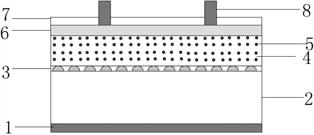
[0038] Specifically, the aforementioned SiN-based x The preparation method of the textured doped silicon quantum dot light-emitting diode device comprises the following steps:

[0039] (1) In clean P with epitaxial layer + Deposit a layer of silver nanometer layer on the P-type silicon substrate 2, and perform rapid thermal annealing treatment to form the silver nanoparticle layer 3. Wherein, the thickness of the silver nanoparticle layer 3 is 30nm to 40nm. The process used can be vacuum evaporation, electron beam evaporation or pulsed laser deposition. The annealing temperature of the rapid thermal annealing treatment is 400-500°C, and the annealing time is 60-120s.

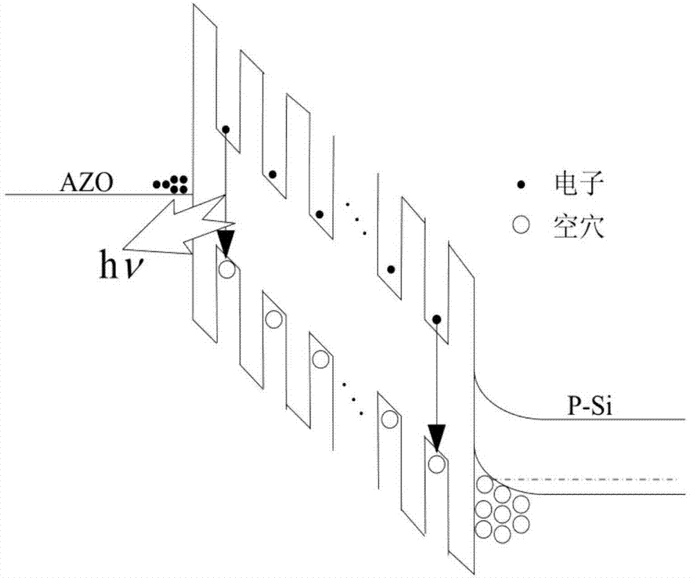
[0040] (2) Alternate deposition of multiple layers of Si on the silver nanoparticle layer 3 3 N 4 layer 4 and doped silicon-rich SiN x Layer 5, made of Si 3 N 4 The distance between layers 4 controls the size of the silicon quantum dots, annealing is performed in an argon environment, and doped silicon q...

example 1

[0047] (1) Use the standard RCA method to clean the P with epitaxial layer + / P-type single crystal silicon substrate 2;

[0048] (2) Form a layer of silver nano-film with a thickness of 30nm on the clean substrate 2 by vacuum evaporation method, and then perform rapid heat treatment to form the silver nano-particle layer 3, wherein the temperature of rapid annealing is 400°C, and the annealing time is 90s;

[0049] (3) Alternating deposition thickness of Si on the silver nanoparticle layer 3 by plasma enhanced chemical vapor deposition (PECVD) technique 3 N 4 Control layer 4 / Silicon-rich SiN doped with phosphorus (P) x Layer 5; deposition 4 into NH 3 (purity is 99.999%) flow rate is 30sccm, by H 2 SiH diluted 10% by volume 4 The flow rate is 60sccm, the deposition time of layer 4 is 15s, and a total of 16 layers are deposited; deposition 5 is fed with NH 3 (purity is 99.999%) flow rate is 10sccm, by H 2 SiH diluted 10% by volume 4 The flow rate is 60sccm, by H 2 PH w...

example 2

[0057] (1) Use the standard RCA method to clean the P with epitaxial layer + / P-type single crystal silicon substrate 2;

[0058] (2) Form a layer of silver nano-film with a thickness of 30nm on the clean substrate 2 by vacuum evaporation method, and then perform rapid heat treatment to form the silver nano-particle layer 3, wherein the temperature of rapid annealing is 400°C, and the annealing time is 90s;

[0059] (3) Alternating deposition thickness of Si on the silver nanoparticle layer 3 by plasma enhanced chemical vapor deposition (PECVD) technique 3 N 4 Control layer 4 / Silicon-rich SiN doped with phosphorus (P) x Layer 5; deposition 4 into NH 3 (purity is 99.999%) flow rate is 30sccm, by H 2 SiH diluted 10% by volume 4 The flow rate is 60sccm, the deposition time of layer 4 is 15s, and a total of 20 layers are deposited; deposition 5 is fed with NH 3 (purity is 99.999%) flow rate is 10sccm, by H 2 SiH diluted 10% by volume 4 The flow rate is 60sccm, by H 2 PH w...


PUM

PropertyMeasurementUnit
thicknessaaaaaaaaaa
thicknessaaaaaaaaaa
diameteraaaaaaaaaa

Abstract

The invention discloses a doped silicon quantum dot light emitting diode device which comprises a silicon substrate, a sedimentary silver nanometer particle layer, a plurality of layers of SiNx films, a transparent electricity conducting film AZO layer and an Si3N4 passivation layer. The SiNx films are deposited on a silver nanometer particle structure, are evenly distributed and contain doped silicon quantum dots. The invention further discloses a preparation method of the light emitting diode. The method comprises the steps of utilizing the electroluminescent characteristic of the doped silicon quantum dot-SiNx films to constitute a light emitting active layer of the light emitting diode, and utilizing doping to passivate quantum dots, and enhancing the radiative recombination of an electron hole through a p-n node formed by the doping silicon quantum dot and the silicon substrate. Further, the silver nanometer structure is used for enhancing the strength of electroluminescence, and the doped silicon quantum dot light emitting diode device improves the light emitting efficiency of a light emitting component and is compatible with the traditional CMOS technology.

Description

technical field [0001] The invention belongs to the technical field of microelectronics and optoelectronics, and more specifically relates to a doped silicon quantum dot light-emitting diode and a preparation method thereof. Background technique [0002] Silicon-based integrated circuits develop at an astonishing speed according to Moore's law. At the same time, the size of lithography is decreasing exponentially year by year. While reducing the size of transistors, more and more transistors are integrated into a chip, making the wiring inside the circuit denser and thinner. According to statistics, for complex chips, the interconnection layer of its wires has reached 12 layers, and the metal connection density has reached 2222m / cm 2 . This will cause problems such as prolonging the response time of the signal, increasing the heat generation, and the signal interference becoming more and more obvious, etc., which will seriously affect the performance of the device in the e...

Claims


Application Information

Patent Timeline
Patent Type & Authority Applications(China)
IPC IPC(8): H01L33/26H01L33/00
CPCH01L33/005H01L33/025H01L33/06H01L33/26
Inventor 曾祥斌廖武刚文西兴郑文俊冯枫文杨阳黄诗涵
Owner HUAZHONG UNIV OF SCI & TECH
Why Eureka
Try Eureka