Microstructure light trapping method for silicon-based thin film solar cell

A technology of solar cells and silicon-based thin films, applied in circuits, photovoltaic power generation, electrical components, etc., can solve the problems of reduced production efficiency and easy puncture of thin film layers, so as to improve efficiency, improve light trapping ability, and increase photoelectric conversion efficiency Effect

Inactive Publication Date: 2014-03-12
SHANGHAI JIAO TONG UNIV
View PDF8 Cites 5 Cited by
  • Summary
  • Abstract
  • Description
  • Claims
  • Application Information

AI Technical Summary

Problems solved by technology

[0007] An invention patent previously applied by the applicant: "Preparation and application of light-trapping structural glass for thin-film solar cells", application number: 201310039891.7, application date: 2013-02-01, the invention discloses a light-trapping The preparation process of the glass sheet, and it is proposed that the thin-film battery can be deposited on the light-trapping surface of the light-trapping glass sheet, but there are two shortcomings in depositing the battery on the light-trapping surface: first, the traditional thin-film battery is deposited on the flat surface Structurally, it is necessary to re-explore the process parameters for the deposition of cells; secondly, due to the existence of the light-trapping structure, the deposited thin film layer is easy to pierce and become a waste product, resulting in a decrease in production efficiency

Method used


Image

  • Microstructure light trapping method for silicon-based thin film solar cell
  • Microstructure light trapping method for silicon-based thin film solar cell
  • Microstructure light trapping method for silicon-based thin film solar cell

Examples


Embodiment 1

[0028] Example 1 (single-junction battery preparation)

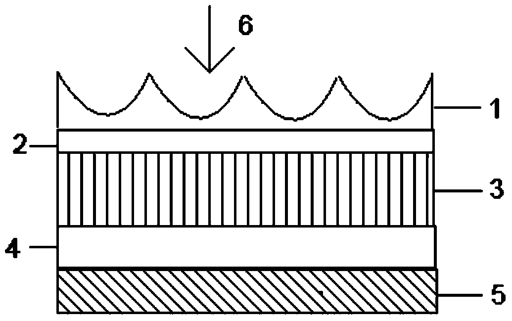
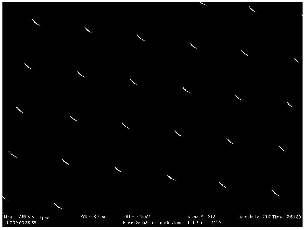
[0029]1. Through photolithography, development and etching, etc., prepare a hemispherical pit structure with a size of 10 μm and periodically arranged on the flat glass suitable for solar cells, as a light-trapping structure for thin-film solar cells.

[0030] 2. Use the light-trapping structural glass prepared in step 1 as the substrate, and deposit 0.3 μm TCO on it as the front electrode.

[0031] 3. Deposit 0.3μm a-Si as the p-i-n structure of the battery.

[0032] 4. Deposit 0.1 μm AZO as the back electrode and transition layer.

[0033] 5. Finally, 0.3 μm Ag is used as the back reflection layer to obtain a single-junction high-efficiency light-trapping thin-film solar cell. The schematic diagram is as follows figure 1 shown.

Embodiment 2

[0034] Example 2 (Double-junction battery preparation)

[0035] 1. On the basis of steps 1-4 of Example 1, deposit 2 μm microcrystalline silicon as the p-i-n structure of the bottom cell.

[0036] 2. Deposit 0.1μm AZO as the back electrode and transition layer.

[0037] 3. Finally, 0.3 μm Ag is used as the back reflection layer to obtain a double-junction high-efficiency light-trapping thin film solar cell.

Embodiment 3

[0038] Example 3 (light-trapping structure covered thin-film battery)

[0039] 1. According to the method shown in Step 1 of Example 1, prepare a light-trapping glass sheet with a size of 10 μm and a size of 2 μm.

[0040] 2. Prepare a thin-film battery according to steps 1-3 of Example 1.

[0041] 3. The 10μm light-trapping glass covers the surface of the battery for anti-reflection, and the 2μm light-trapping glass covers the bottom of the battery, which can effectively improve the absorption rate of infrared and near-infrared photons.

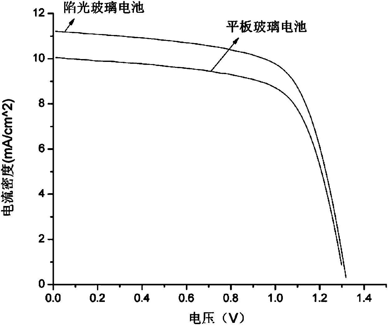
[0042] In the above implementation, first prepare a micron-scale light-trapping glass sheet, and then use the light-trapping glass sheet as a substrate to deposit a thin-film battery, or cover the light-trapping glass sheet on the thin-film battery, which can effectively improve the light absorption of the thin-film battery. Thereby improving battery efficiency. The light-trapping glass sheet is used as the substrate of the thin-film batte...


PUM


Abstract

The invention relates to a microstructure light trapping method for a silicon-based thin film solar cell. A micrometer-scale periodic structure is used as a light trapping part of the cell, or the micrometer-scale periodic structure and a textured structure form the light trapping part of the cell. The light trapping structure is prepared on a substrate material, and the thin film solar cell can be directly deposited on the light trapping substrate, and can be covered by light trapping sheet glass, so that the light trapping capability of the cell can be effectively improved, the photo absorption can be improved, and the photoelectric conversion efficiency of the thin film solar cell can be improved. Photoelectric efficiency tests show that the relative efficiency of a double-junction amorphous silicon/microcrystalline silicone cell can be improved by 9.95 percent by the light trapping technology. The microstructure light trapping method is compatible with a conventional thin film cell preparation technology, and is suitable for large-area batch production, and the efficiency of the thin film solar cell can be effectively improved under the condition of no changes in process parameters.

Description

technical field [0001] The invention relates to the fields of micro-nano processing, energy technology and optoelectronic devices, in particular to a silicon-based thin-film solar cell light-trapping technology. Background technique [0002] Entering the 21st century, with the rapid development of the global economy, human demand for energy continues to increase, and traditional fossil energy is increasingly exhausted. At the same time, the large amount of waste gas produced by fossil energy is deteriorating our living environment. In order to deal with the energy crisis and environmental pollution, it is necessary to develop and utilize renewable, clean and pollution-free new energy, and follow the path of sustainable development to ensure a stable and lasting energy supply for human beings. The sun radiates energy continuously through the fusion of hydrogen nuclei. The energy irradiated to the earth every second is equivalent to the heat produced by burning 5 million tons...

Claims


Application Information

Patent Timeline
Patent Type & Authority Applications(China)
IPC IPC(8): H01L31/20
CPCH01L31/02167H01L31/02327Y02E10/50Y02P70/50
Inventor 王庆康沈向前王阳培华黄堃严兴茂
Owner SHANGHAI JIAO TONG UNIV
Why Eureka
Try Eureka