Rapid cross section manufacture and sub-surface micro-crack detection method of single crystal semiconductor substrate

A single crystal semiconductor and detection method technology, which is applied in the preparation of test samples, optical test flaws/defects, etc., can solve problems such as low efficiency and complex production methods, and can ensure accuracy, intuitive detection results, and position accuracy. Effect

Active Publication Date: 2014-03-19
GUANGDONG UNIV OF TECH
View PDF9 Cites 14 Cited by
  • Summary
  • Abstract
  • Description
  • Claims
  • Application Information

AI Technical Summary

Problems solved by technology

Most domestic and foreign scholars use sandpaper grinding, polishing and corrosion methods to make cross-sectional samples, such as the literature H. H. K. Xu, S. Jahanmir. Simple techn...

Method used


Image

  • Rapid cross section manufacture and sub-surface micro-crack detection method of single crystal semiconductor substrate
  • Rapid cross section manufacture and sub-surface micro-crack detection method of single crystal semiconductor substrate
  • Rapid cross section manufacture and sub-surface micro-crack detection method of single crystal semiconductor substrate

Examples


Embodiment 1

[0028] In this embodiment, the detection of subsurface microcracks is carried out on the single crystal SiC substrate obtained under the grinding conditions of 325# diamond grinding wheel, the workpiece rotation speed is 151rpm, the grinding wheel rotation speed is 3000rpm, and the grinding wheel feed speed is 5 μm / s. include:

[0029] Step 1: Put the ground single-crystal SiC substrate into acetone for ultrasonic cleaning for 5 minutes, then put it into deionized water for 2 minutes, and finally put it into a dryer for drying.

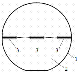
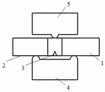
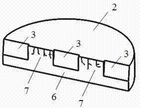
[0030] Step 2: If figure 1 As shown, the single crystal SiC substrate is placed on the center of the workbench of the UVCAS-5W-B semi-automatic wafer cutting machine with the grinding surface facing up, and three micro-grooves 3 are processed along the same straight line direction of the surface to be tested 2, The actual output current value of the power supply of the wafer laser cutting machine is 40A, the cutting speed is 1mm / s, and the micro groo...

Embodiment 2

[0034] In this embodiment, the detection of subsurface microcracks is carried out on the single crystal SiC substrate obtained under the grinding conditions of 8000# diamond grinding wheel, the workpiece rotation speed is 151rpm, the grinding wheel rotation speed is 3000rpm, and the grinding wheel feed speed is 0.1 μm / s. Steps include:

[0035] Step 1: put the ground single crystal SiC substrate into alcohol for ultrasonic cleaning for 5 minutes, then put it into deionized water for 2 minutes, and finally put it into a dryer for drying.

[0036] Step 2: If figure 1 As shown, the single crystal SiC substrate is placed on the center of the workbench of the UVCAS-5W-B semi-automatic wafer cutting machine with the grinding surface facing up, and two micro-grooves 3 are processed along the same straight line direction of the surface to be tested 2, and the The actual output current value of the power supply of the wafer laser cutting machine is 35A, the cutting speed is 0.5mm / s, a...

Embodiment 3

[0040] In this embodiment, subsurface microcrack detection is carried out on a single crystal SiC substrate obtained by grinding under the process conditions of a loading weight of 3080g, a grinding disc rotation speed of 80rpm, and a processing time of 30min with W14 diamond abrasive, and the steps include:

[0041] Step 1: Put the ground single-crystal SiC substrate into electronic cleaner DZ-1 for ultrasonic cleaning for 5 minutes, then put it in deionized water for 2 minutes, and finally put it in a dryer for drying.

[0042] Step 2: If figure 1 As shown, the single crystal SiC substrate is placed on the center of the workbench of the UVCAS-5W-B semi-automatic wafer cutting machine with the grinding surface facing up, and two micro-grooves 3 are processed along the same straight line direction of the surface to be tested 2, and the wafer The actual output current value of the power supply of the circular laser cutting machine is 30A, the cutting speed is 0.1mm / s, and the m...


PUM

PropertyMeasurementUnit
Thicknessaaaaaaaaaa

Abstract

The invention relates to a rapid cross section manufacture and sub-surface micro-crack detection method of a single crystal semiconductor substrate. The method comprises the steps of cleaning the single crystal semiconductor substrate; processing one micro-groove or more micro-grooves on the single crystal semiconductor substrate along the direction of the same straight line of the surface to be detected; applying pressure onto the crack of the back(s) of the more micro-groove(s) of the single crystal semiconductor substrate, and enabling the single crystal semiconductor substrate to be broken into two along the direction(s) of the micro-groove(s) under the action of the force to complete sample preparation of the cross section of the single crystal semiconductor substrate; horizontally putting the detected cross section of the broken single crystal semiconductor substrate under an optical microscope and observing; moving the single crystal semiconductor substrate to enable the boundary between the surface to be detected and the detected cross section to appear in a visual area; adjusting the multiplying power of a lens of the optical microscope, and shooting the optical micrograph of a target area on the cross section; and measuring the maximum distance between the crack on the detected cross section and the boundary between the surface to be detected and the detected cross section to complete the sub-surface micro-crack detection work of the single crystal semiconductor substrate. The rapid cross section manufacture and sub-surface micro-crack detection method is feasible and dependable in detection result.

Description

technical field [0001] The invention relates to the technical field of detection of subsurface microcracks in the processing of single crystal semiconductor substrates, in particular to the cross-section preparation of superhard semiconductor substrates such as single crystal silicon, single crystal sapphire and single crystal SiC, and a detection method for subsurface microcracks. Background technique [0002] The rapid development of modern electronics and optoelectronic technology has driven the development of semiconductor materials for making related devices, such as the research, development and application of single crystal semiconductor materials silicon, sapphire and silicon carbide. Silicon carbide (SiC), as the third-generation wide-bandgap semiconductor material, has the advantages of wide bandgap, high thermal conductivity, high breakdown field strength, high saturation electron drift rate and high bonding energy, etc. Its excellent performance can meet the requi...

Claims


Application Information

Patent Timeline
IPC IPC(8): G01N1/28G01N21/88
Inventor 潘继生陈森凯路家斌阎秋生
Owner GUANGDONG UNIV OF TECH
Why Eureka
Try Eureka