Photoconductive switch manufacturing method based on SiC substrate

A technology for a photoconductive switch and a manufacturing method, which is applied in the direction of semiconductor devices, final product manufacturing, sustainable manufacturing/processing, etc., can solve the problem that the photoconductive switch cannot meet the performance requirements of high power, ultra-high speed, thermal stability, etc., and achieves a reduction in production. Cost, reduce process flow, improve the effect of yield

Inactive Publication Date: 2014-03-26
SHANGHAI NORMAL UNIVERSITY
View PDF2 Cites 17 Cited by
  • Summary
  • Abstract
  • Description
  • Claims
  • Application Information

AI Technical Summary

Problems solved by technology

[0004] However, the semi-insulating GaAs crystal-based photoconductive switch still cannot meet the high-power, ultr...

Method used


Image

  • Photoconductive switch manufacturing method based on SiC substrate
  • Photoconductive switch manufacturing method based on SiC substrate

Examples


Embodiment Construction

[0012] Below in conjunction with accompanying drawing and embodiment the present invention is described in further detail

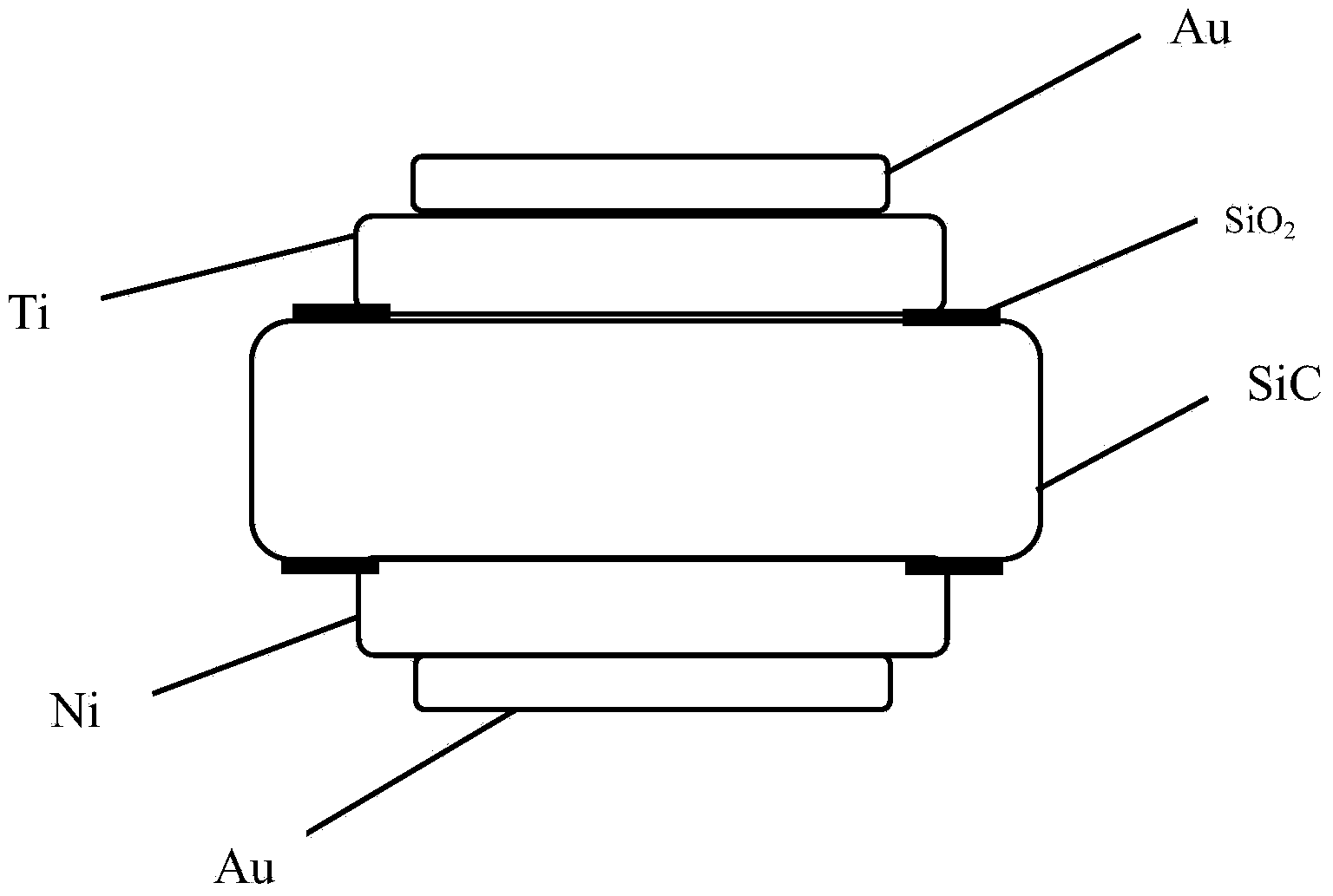
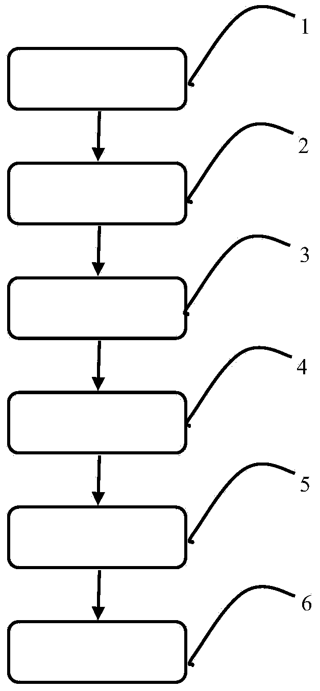
[0013] A method for manufacturing a photoconductive switch based on a SiC substrate according to the present invention (as shown in the attached figure 1 , 2 shown), including the following steps:

[0014] Step 1, SiC substrate: the substrate is a SiC wafer, cleaned by a standard semiconductor process.

[0015] Step 2, SiO 2 Insulation protective layer: Wet oxygen is passed into the tube furnace, 10-25sccm, temperature 1200-1350℃, oxidized to SiO at constant temperature for 5-10 hours 2 film; then open the window by photolithography, and use the microelectronics dry etching process RIE Ar high-energy ions to roughen the substrate surface.

[0016] Step 3, preparing Ti electrode thin film: using high vacuum magnetron sputtering equipment, depositing a layer of Ti electrode thin film, the thickness of which is controlled at 100-140nm.

[0017] Step 4, ...


PUM

PropertyMeasurementUnit
Thicknessaaaaaaaaaa
Thicknessaaaaaaaaaa

Abstract

The invention provides a photoconductive switch manufacturing method based on a SiC substrate, and relates to the technical field of wide bandgap semiconductor material photoelectronic devices. SiC with the thickness of 400 micrometers after polishing serves as a substrate in the photoconductive switch manufacturing method based on the SiC substrate. The photoconductive switch manufacturing method based on the SiC substrate comprises the steps that the SiC substrate is prepared; a SiO2 insulation protective layer is generated through thermal oxidation, and a window is formed through photoetching; in high vacuum low temperature Ar atmosphere, a Ti electrode is deposited on the carbon surface, and a Ni electrode is deposited on the silicon surface; after high temperature rapid thermal processing in the Ar atmosphere, a Au protective film is deposited through a small-size ion sputtering instrument, and a photoconductive switch of a Au/Ti/SiC/Ni/Au different-surface opposite-electrode structure is formed by being encapsulated through transparent Si3N4 after a copper electrode is bonded. According to the photoconductive switch manufacturing method based on the SiC substrate, due to the fact that epitaxy of an n-type or p-type SiC epitaxial layer with high doping concentration is not carried out through devices such as CVDs, the technological process of semiconductors is reduced, the rate of finished products is improved, and production cost is lowered. Technical assurance is provided for the production of devices having hash requirements for large power, high frequency and high temperature resistance in future.

Description

technical field [0001] The invention relates to the technical field of wide-bandgap semiconductor material optoelectronic devices, and specifically refers to a method for manufacturing a photoconductive switch based on a SiC substrate with high frequency, high power, high temperature resistance and anti-interference. Background technique [0002] In the semiconductor industry, Si has been developed as a dominant semiconductor device for nearly half a century. In 1975, D.H.Auston and others successfully developed the first photoconductive switch, which was based on high resistance Si crystal (10 4 Ω·cm) is realized as the base material. In 1982, C.S.Chang et al. of the University of Maryland made a ps-level Blumlein pulse transmitter using a high-resistance Si crystal as a substrate for a photoconductive switch. Since the band gap of Si single crystal is only 1.12eV, the intrinsic excitation can also generate a certain number of carriers at room temperature. Therefore, even...

Claims


Application Information

Patent Timeline
IPC IPC(8): H01L31/18H01L31/0224H01L31/08
CPCH01L31/022408H01L31/09H01L31/1812Y02P70/50
Inventor 张永平卢吴越谈嘉慧程越赵高杰孙玉俊刘益宏陈恩龙李万荣陈之战石旺舟
Owner SHANGHAI NORMAL UNIVERSITY
Why Eureka
Try Eureka