Organic light-emitting device and preparation method thereof

An electroluminescent device and luminescent technology, which is applied in the fields of electric solid-state devices, semiconductor/solid-state device manufacturing, electrical components, etc., can solve problems such as poor blocking effect, small size of alkali metal ions, and exciton quenching

Inactive Publication Date: 2014-03-26
OCEANS KING LIGHTING SCI&TECH CO LTD +2
View PDF0 Cites 4 Cited by
  • Summary
  • Abstract
  • Description
  • Claims
  • Application Information

AI Technical Summary

Problems solved by technology

For the N-doping of the electron transport layer, alkali metal compounds are usually used for doping. This is due to the low work function of alkali metals and the N-doping effect is easy to achieve, but the alkali metal ions are small in size and strong in diffusion ability. The diffusion distance in the medium is long, and the alkali metal ions may diffuse into the light-emitting layer in addition to being doped in the transport layer, which directly leads to the quenching of excitons and affects the light efficiency and life of the device.
[0004] Traditional organic electroluminescent devices use electron transport materials, such as Bphen, as the hole blocking layer. However, the film quality of traditional electron transport materials is poor, resulting in poor blocking effect, which affects the performance of organic electroluminescent devices. Luminous efficiency

Method used


Image

  • Organic light-emitting device and preparation method thereof
  • Organic light-emitting device and preparation method thereof
  • Organic light-emitting device and preparation method thereof

Examples


preparation example Construction

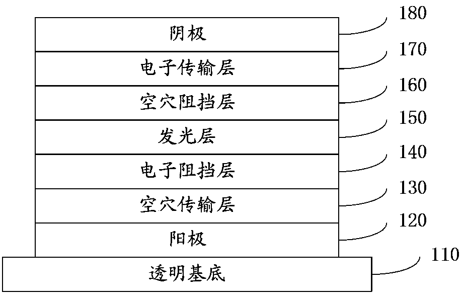
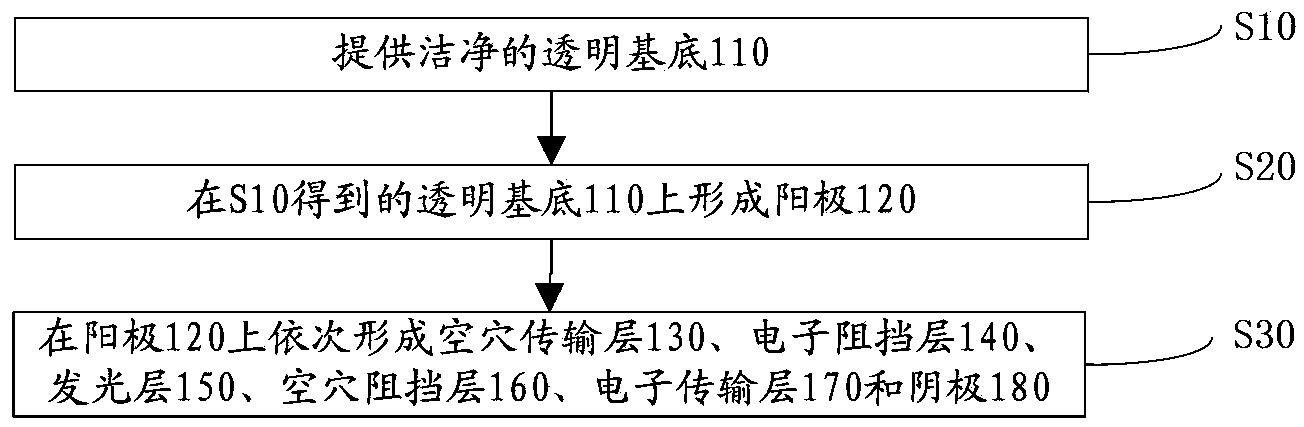
[0065] Such as figure 2 The preparation method of the above-mentioned organic electroluminescence device shown, comprises the following steps:

[0066] S10 , providing a clean transparent substrate 110 .

[0067] The transparent substrate 110 can be common glass. The transparent substrate 110 was ultrasonically cleaned in deionized water containing detergent, and then ultrasonically treated in isopropanol and acetone for 20 minutes, and then dried with nitrogen to obtain a clean transparent substrate 110 .

[0068] S20, forming an anode 120 on the transparent substrate 110 obtained in S10.

[0069] The anode 120 is formed on the transparent substrate 110 by magnetron sputtering system.

[0070] The anode 120 can be an ITO thin film or an AZO thin film, and the thickness can be 70nm~200nm.

[0071] S20 also includes the operation of placing the transparent substrate 110 formed with the anode 120 in a plasma processing chamber for plasma processing. Performing plasma treatme...
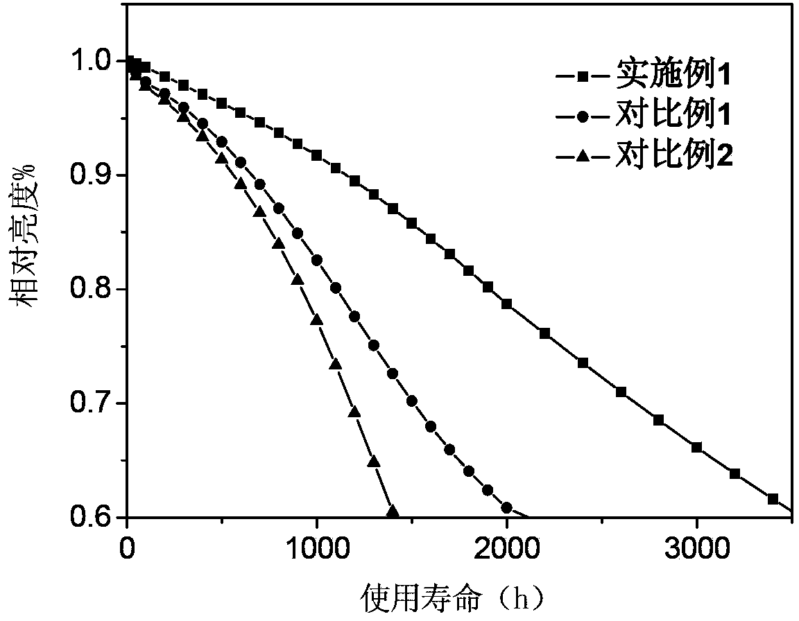
Embodiment 1

[0095] The transparent substrate was ultrasonically cleaned in deionized water containing detergent. After cleaning, it was ultrasonically treated in isopropanol and acetone for 20 min, and then dried with nitrogen to obtain a clean transparent substrate.

[0096] The anode is formed on the transparent substrate by magnetron sputtering, the material of the anode is AZO, and the thickness of the anode is 70nm. The transparent substrate formed with the anode is placed in a plasma treatment chamber for plasma treatment.

[0097] In a vacuum of 5 x 10 -4 In the vacuum coating system of Pa, a hole transport layer with a thickness of 60nm is formed on the anode by evaporation. The material of the hole transport layer is MeO-TPD doped with F6-TNAP. F6-TNAP accounts for the mass of the hole transport layer. The percentage is 5%.

[0098] In a vacuum of 5 x 10 -4 In Pa's vacuum coating system, an electron blocking layer with a thickness of 5nm is evaporated on the hole transport layer...

Embodiment 2

[0106] The transparent substrate was ultrasonically cleaned in deionized water containing detergent. After cleaning, it was ultrasonically treated in isopropanol and acetone for 20 min, and then dried with nitrogen to obtain a clean transparent substrate.

[0107] The anode is formed on the transparent substrate by magnetron sputtering, the material of the anode is ITO, and the thickness of the anode is 100 nm. The transparent substrate formed with the anode is placed in a plasma treatment chamber for plasma treatment.

[0108] In a vacuum of 5 x 10 -4 In the vacuum coating system of Pa, a hole transport layer with a thickness of 60nm is formed on the anode by evaporation. The material of the hole transport layer is MeO-TPD doped with F6-TNAP. F6-TNAP accounts for the mass of the hole transport layer. The percentage is 5%.

[0109] In a vacuum of 5 x 10 -4 In Pa's vacuum coating system, an electron blocking layer with a thickness of 5nm is evaporated on the hole transport l...


PUM


Abstract

The invention discloses an organic light-emitting device which comprises a transparent substrate, an anode, a hole transfer layer, an electron blocking layer, a light emitting layer, a hole blocking layer, an electron transfer layer and a cathode which are sequentially stacked, wherein the hole blocking layer is made from an organometallic complex, the ligand of the organometallic complex is hydroxyquinoline, hydroxyquinoline derivative, hydroxyl benzoquinoline or hydroxyl benzoquinoline derivative. The hole blocking layer of the organic light-emitting device is made from an organometallic complex, the film formation quality of the organometallic complex is good so as to be good for preventing the diffusion of a hole to the light emitting layer, and compared with a traditional organic light-emitting device, the luminous efficiency is improved. The invention further provides a preparation method of the organic light-emitting device.

Description

technical field [0001] The invention relates to the field of light-emitting devices, in particular to an organic electroluminescent device and a preparation method thereof. Background technique [0002] Organic electroluminescent diodes have a sandwich-like structure, with a cathode and an anode at the top and bottom, and a single or multiple functional layers of organic materials of different materials and structures sandwiched between the two electrodes, followed by hole injection. layer, hole transport layer, light emitting layer, electron transport layer, electron injection layer. The organic electroluminescent device is a carrier-injection light-emitting device. After the anode and the cathode are applied with an operating voltage, holes are injected from the anode and electrons from the cathode into the organic material layer of the working device respectively. Hole-electron pairs are formed in the luminescent material to emit light, and then the light is emitted from...

Claims


Application Information

Patent Timeline
Patent Type & Authority Applications(China)
IPC IPC(8): H01L51/50H01L51/54H01L51/56
CPCH10K71/10H10K85/326H10K85/324H10K85/381H10K50/18
Inventor 周明杰王平冯小明陈吉星
Owner OCEANS KING LIGHTING SCI&TECH CO LTD
Why Eureka
Try Eureka