Organic light-emitting device and preparation method thereof
An electroluminescent device and a luminescent technology, which are applied in the direction of organic semiconductor devices, the manufacture/processing of organic semiconductor devices, and electric solid-state devices, etc., can solve the problems of low light extraction performance, total reflection loss, and poor refractive index, etc., and achieve light output. high efficiency effect
- Summary
- Abstract
- Description
- Claims
- Application Information
AI Technical Summary
Problems solved by technology
Method used
Image

Examples
preparation example Construction
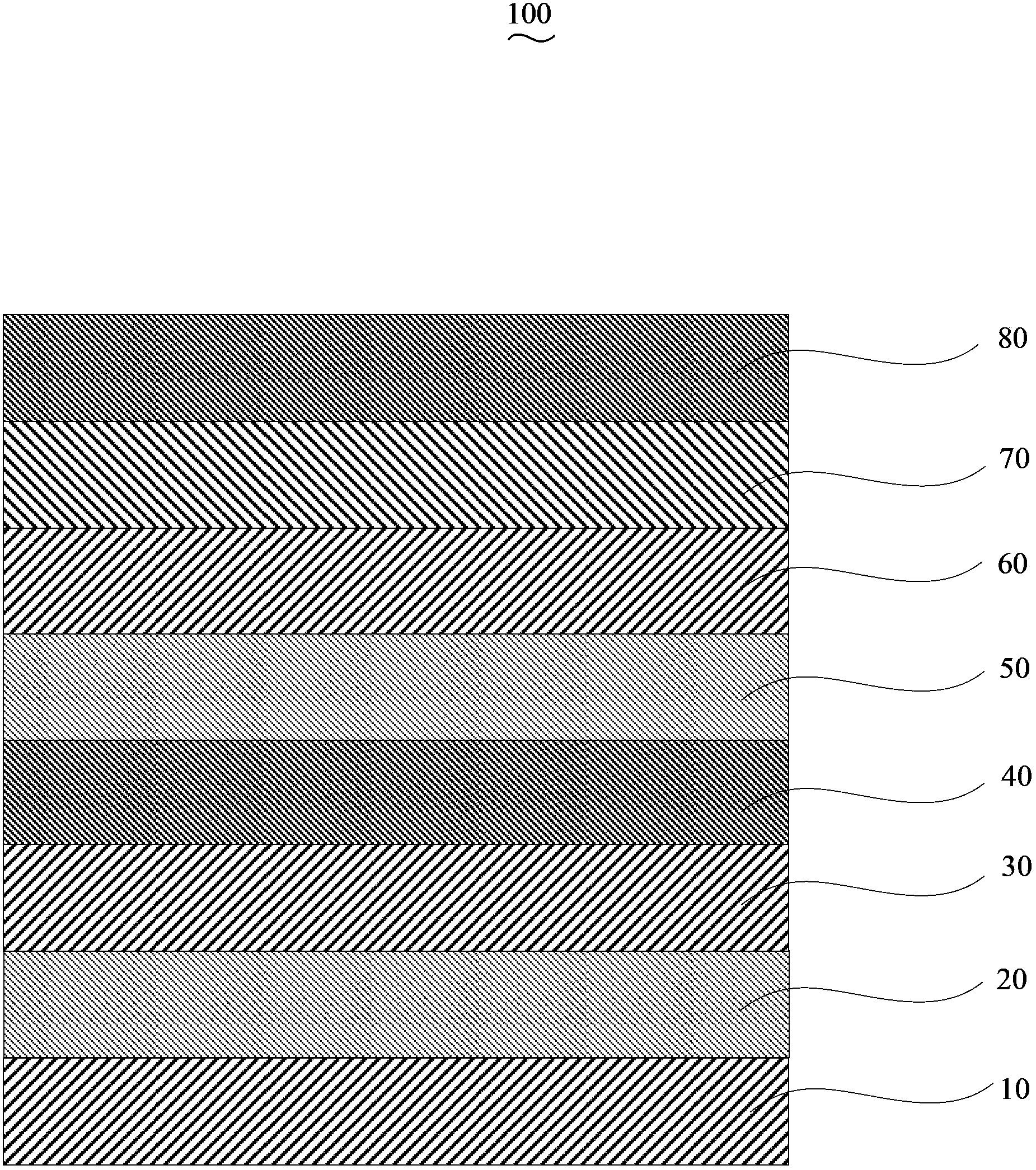
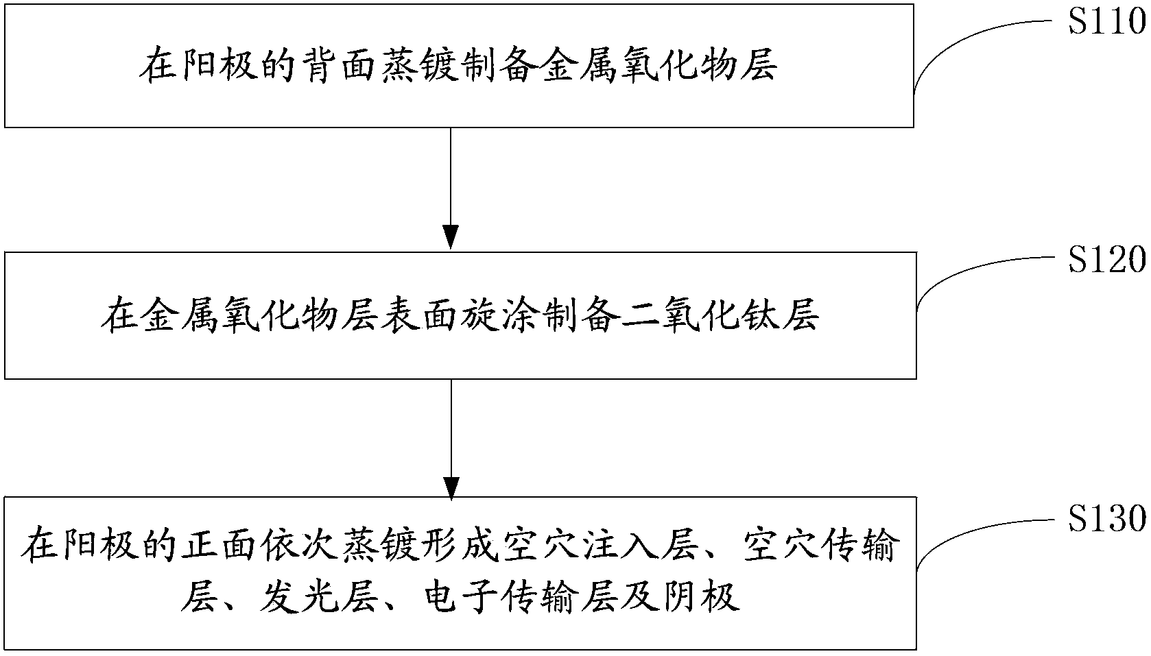
[0034] Please also see figure 2 , the preparation method of the organic electroluminescent device 100 of an embodiment, it comprises the following steps:
[0035] Step S110 , preparing the metal oxide layer 20 on the back surface of the anode 30 by vapor deposition.
[0036] The anode 30 is indium tin oxide glass (ITO), aluminum zinc oxide glass (AZO) or indium zinc oxide glass (IZO), preferably ITO. A conductive layer is formed on one side of the anode 30 , the side on which the conductive layer is formed is the front side, and the side on which the conductive layer is not formed is the back side.
[0037] In this embodiment, the anode 30 is pretreated before the metal oxide layer 20 is vapor-deposited on the back surface of the anode 30 . The pretreatment of the anode 30 is as follows: the anode 30 is first subjected to photolithography treatment, cut into the required size, and then ultrasonically cleaned with detergent, deionized water, acetone, ethanol, and isopropanon...
Embodiment 1
[0053] The structure prepared in this example is TiO 2 / MoO 3 / ITO glass / V 2 o 5 / NPB / ADN / TAZ / Ag organic electroluminescent devices.
[0054] First use detergent, deionized water, and ultrasonic for 15 minutes to remove the organic pollutants on the glass surface, then prepare a scattering layer on the back of the conductive anode substrate (the side in contact with the air), and first evaporate the metal oxide layer , the material is MoO 3 , with a thickness of 25nm, and then spin-coated to prepare a titanium dioxide layer, TiO 2 Firstly, it is calcined at 450 degrees for 30 minutes, and then it is ground into powder and configured into a solution with a mass fraction of 35%, and the solvent is water. Add 5ml of acetylacetone, 2ml of triton, stir well, then spin coat on MoO 3 On top, dried to a thickness of 15 μm. Evaporated hole injection layer: the material is V 2 o 5 , with a thickness of 30nm; evaporated hole transport layer: the material is NPB, with a thickness...
Embodiment 2
[0059] The structure prepared in this example is TiO 2 / CaO / AZO glass / WO 3 / TCTA / Alq 3 / TPBi / Au organic electroluminescent devices.
[0060] Firstly, the AZO glass substrate is washed with detergent, deionized water, and ultrasonic for 15 minutes to remove organic pollutants on the glass surface, and then a scattering layer is prepared on the back of the conductive anode substrate, and a metal oxide layer is prepared by evaporation. The material is CaO, the thickness 10nm, and then spin-coated to prepare a titanium dioxide layer, TiO 2 Firstly, it is calcined at 400 degrees for 60 minutes, and then it is ground into powder and configured into a solution with a mass fraction of 50%, and the solvent is n-butanol. Add 10ml of acetylacetone and 1ml of Triton, stir well, then spin-coat on CaO, then dry, with a thickness of 30μm. Evaporated hole injection layer: the material is WO 3 , with a thickness of 20nm; evaporated hole transport layer: the material is TCTA, with a thickn...
PUM
| Property | Measurement | Unit |
|---|---|---|
| thickness | aaaaa | aaaaa |
| thickness | aaaaa | aaaaa |
| particle diameter | aaaaa | aaaaa |
Abstract
Description
Claims
Application Information