
One-dimensional organic semiconductor nanowire with fluorescence and photoconduction dual response for organic amine gas as well as preparation method and application of nanowire

An organic semiconductor and photoconductive technology, applied in fluorescence/phosphorescence, chemical instruments and methods, organic chemistry, etc., can solve problems such as low carrier mobility, fluorescence quenching, and difficulties in organic semiconductor nanomaterials

Active Publication Date: 2014-04-09
INST OF CHEM CHINESE ACAD OF SCI
View PDF3 Cites 32 Cited by
  • Summary
  • Abstract
  • Description
  • Claims
  • Application Information

AI Technical Summary

Problems solved by technology

It is very difficult to prepare organic semiconductor nanomaterials with high fluorescence emission efficiency and electrical conductivity (carrier mobility) at the same time
On the one hand, the reason is that these two properties are mutually exclusive. Generally, to obtain high carrier mobility, a strong π-π overlap between adjacent nanowires is required, but this easily leads to fluorescence quenching; on the other hand, To obtain materials with high fluorescence quantum yield (≥20%), it is usually necessary to disperse the building monomer molecules based on the strong π-π interaction and reduce the π-π interaction between the building monomer molecules. However, this will lead to Flow rate is not high

Method used


Image

  • One-dimensional organic semiconductor nanowire with fluorescence and photoconduction dual response for organic amine gas as well as preparation method and application of nanowire
  • One-dimensional organic semiconductor nanowire with fluorescence and photoconduction dual response for organic amine gas as well as preparation method and application of nanowire
  • One-dimensional organic semiconductor nanowire with fluorescence and photoconduction dual response for organic amine gas as well as preparation method and application of nanowire

Examples


Embodiment 1

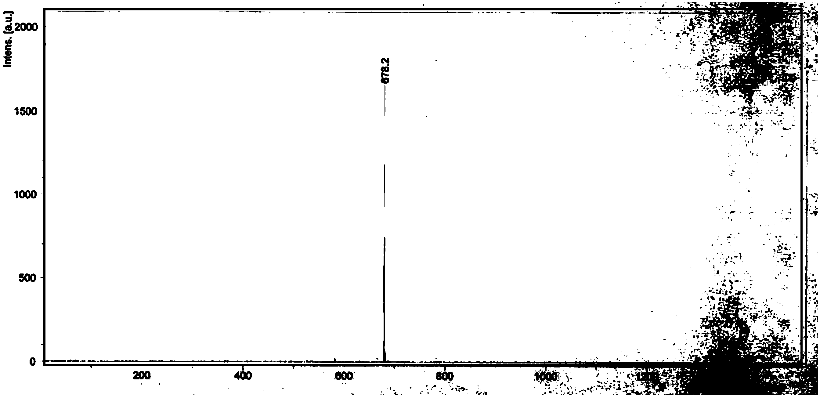
[0050] (1) Mix 50-100 mg of perylene-3,4,9,10-tetracarboxylic dianhydride and 8 g of imidazole, heat to 130°C to dissolve, then inject slowly into dodecylamine for 3 hours of reaction The reaction solution was obtained, and then 10 ml of ethanol and 15 ml of concentrated hydrochloric acid (36% in mass concentration) were added to the reaction solution and stirred overnight; the product was taken out, rinsed with water until the pH was neutral, and then dried for use;

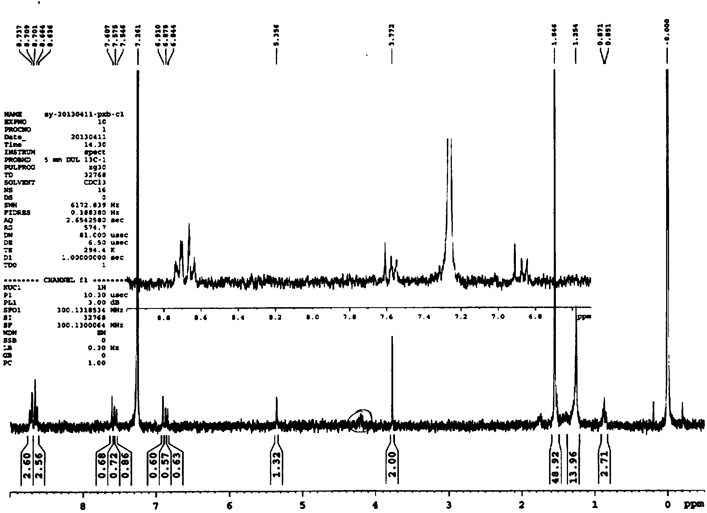
[0051] (2) Take 50 mg of the product obtained after drying in step (1), add 8 g of imidazole and 200 microliters of p-methoxybenzylamine to it, and react at a temperature of 130 ° C for 3 hours to obtain a reaction solution , then add 15 milliliters of concentrated hydrochloric acid (mass concentration is 36%) to the reaction solution, stir overnight, take out the product, and obtain the amphiphilic perylene imide derivative containing perylene anhydride as shown in the following structure; this containing peryle...

Embodiment 2

[0059] (1) Step (1) of the synthesis method is the same as step (1) of Example 1.

[0060] (2) Take 50 mg of the product obtained after drying in step (1), add 8 g of imidazole and 200 microliters of 3,5-dimethoxybenzylamine to it, and react at a temperature of 130 ° C for 3 hours Obtain the reaction liquid, then add 15 milliliters of concentrated hydrochloric acid (mass concentration: 36%) to the reaction liquid, stir overnight, take out the product, and obtain the amphiphilic perylene imide derivative containing perylene anhydride as shown in the following structure;

[0061]

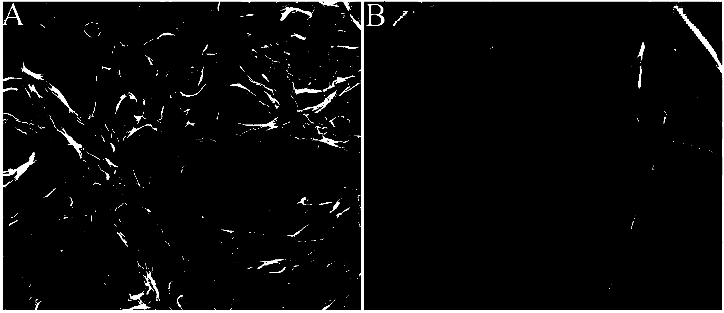
[0062] (3) Dissolve the amphiphilic perylene imide derivative containing perylene anhydride obtained in step (2) in chloroform, then add ethanol (the volume ratio of chloroform to ethanol is 1:1), let it stand still, and prepare multiple The amphiphilic perylene imide derivatives of anhydrides are self-assembled through the π-π interaction between the perylene anhydrides to obtain dark blue one-dim...

Embodiment 3

[0066] The organic amine vapor in the air is detected by using the porous membrane of a plurality of red one-dimensional organic semiconductor nanowires self-assembled and woven to form a network structure prepared in Example 1; wherein: the concentration of n-hexylamine vapor is 50-70ppm; dibutylamine The concentration of steam is 10-20ppm; the concentration of triethylamine vapor is 330-360ppm, 3000-3500ppm respectively; the concentration of o-toluidine vapor is 2-8ppm; the concentration of aniline vapor is 3-8ppm.

[0067] A porous membrane composed of a plurality of red one-dimensional organic semiconductor nanowires self-assembled and woven to form a network structure is placed on a silicon dioxide sheet, so that the surface area of ​​the porous membrane is very large, which is very suitable for gas molecules to flow on the porous membrane. Maximizes adsorption and facilitates diffusion and aggregation. The detected organic amine vapors are n-hexylamine with a concentrati...


PUM

PropertyMeasurementUnit
Particle sizeaaaaaaaaaa
Lengthaaaaaaaaaa

Abstract

The invention relates to a one-dimensional organic semiconductor nanowire with fluorescence and photoconduction dual response for organic amine gas and a preparation method and application of the nanowire. The preparation method comprises the following steps of synthesizing a 3,4,9,10-perylenetetracarboxylic acid anhydride containing amphipathic perylene bisimide derivative to be used as a structure unit; preparing a plurality of 3,4,9,10-perylenetetracarboxylic acid anhydride containing amphipathic perylene bisimide derivatives through a mixed solution of a good solvent and a poor solvent; and carrying out self assembling under the interaction of pi-pi of 3,4,9,10-perylenetetracarboxylic acid anhydride to obtain the one-dimensional organic semiconductor nanowire. When a reticular structural porous membrane formed by knitting the one-dimensional organic semiconductor nanowire is in contact with organic amine steam, the fluorescence is quenched; when the reticular structural porous membrane is in contact with organic fatty amine steam, the photoconduction is enhanced; when the reticular structural porous membrane is in contact with organic aromatic amine steam, the photoconduction is reduced; according to the fluorescence and photoconduction response result, the reticular structural porous membrane formed by knitting the one-dimensional organic semiconductor nanowire can selectively distinguish organic fatty amine and organic aromatic amine.

Description

technical field [0001] The invention belongs to organic semiconductor nanomaterials, and in particular relates to a one-dimensional organic semiconductor nanowire with high fluorescence quantum yield (up to 35%) and high photoconductivity (nanoampere level) which has both fluorescence and photoconductivity responses to organic amine gases and its preparation method; and the application of the one-dimensional organic semiconductor nanowire. technical background [0002] Organic semiconductor nanomaterials have many advantages that inorganic nanomaterials do not have. For example, the structure of organic semiconductor nanomaterials can be adjusted, and they can be prepared by flexible synthesis methods. The manufacturing cost of materials is low, and they are easy to process in large areas. Applied to flexible substrates, etc. Therefore, although organic semiconductor nanomaterials started relatively late compared with inorganic nanomaterials, they have developed rapidly in ...

Claims


Application Information

Patent Timeline
IPC IPC(8): C07D471/06C09K11/06G01N21/64
CPCC07D471/06C09K11/06C09K2211/1029G01N21/643G01N2021/6432
Inventor 车延科张一帆周子超籍宏伟赵进才
Owner INST OF CHEM CHINESE ACAD OF SCI
Learn More