GaN-based light emitting diode and preparation method thereof

A light-emitting diode, gallium nitride-based technology, applied to electrical components, circuits, semiconductor devices, etc., can solve problems such as electrodes, reduce production costs, reduce process steps, and avoid complex interface conditions.

Inactive Publication Date: 2014-04-09
XI AN JIAOTONG UNIV
View PDF5 Cites 3 Cited by
  • Summary
  • Abstract
  • Description
  • Claims
  • Application Information

AI Technical Summary

Problems solved by technology

This process requires the use of chemical vapor deposition, photolithography, and wet etching to prepare a dielectric material layer with a certain thickness on the surface of gallium nitride under the electrode, such as silicon nitride or silicon oxide; due to the multi-interface characteristics of this position Its surface condition is relatively complicated. If the process is not handled properly, it is easy to cause a series of abnormalities in mass production, such as large-area drop-off of electrodes, and cause irreparable losses.

Method used


Image

  • GaN-based light emitting diode and preparation method thereof
  • GaN-based light emitting diode and preparation method thereof

Examples


Embodiment Construction

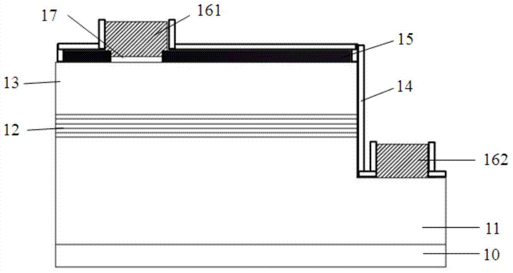
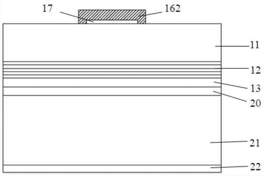
[0027] The present invention will be further described below in conjunction with the accompanying drawings.

[0028] The preparation method of a gallium nitride-based light-emitting diode of the present invention uses photolithography and plasma dry etching technology to carry out surface treatment on the area under the P-type electrode of the LED chip, making it a high-resistance area to obtain a current blocking effect, so that The current flows through other low-resistance regions of the P-type gallium nitride layer, which reduces the loss of luminescence caused by the shading effect in this electrode region, indirectly improves the luminescence of other regions, and uses aluminum mirrors or silver mirrors as part of the metal structure of the P electrode , so as to achieve the purpose of high-efficiency light emission, the preparation method at least includes the following steps:

[0029] 1) Using MOCVD (Metal-organic Chemical Vapor Deposition, metal-organic compound chemi...


PUM


Abstract

The invention discloses a GaN-based light emitting diode and a preparation method thereof. The GaN-based light emitting diode includes an X type GaN layer and an X type electrode arranged on the X type GaN layer; a current obstruction area is formed on the X type GaN layer under the X type electrode; the area of the current obstruction area is smaller than that of the X type electrode; and the X type GaN layer is an N type GaN layer or a P type GaN layer, and the X type electrode corresponding to the X type GaN layer is an N type electrode or a P type electrode. The preparation method uses photoetching and plasma dry etching technology, enables a processed surface to from a high-resistance area, finally achieves the purpose of branching guidance of current, and enables invalid light emission of an LED electrode area is greatly reduced.

Description

Technical field: [0001] The invention belongs to the technical field of gallium nitride-based light-emitting diode manufacturing technology, and specifically relates to a gallium nitride-based light-emitting diode and a preparation method thereof. Background technique: [0002] Light Emitting Diode (LED for short) has been developed for decades, and has been widely used in the fields of signal display, backlight and solid-state lighting, bringing various conveniences to human life. LED devices based on III-V compound gallium nitride (GaN) materials (including various alloy material systems obtained by doping its congeners In and Al elements) can cover most of the wavelength bands from deep ultraviolet to visible light. Most LED devices are manufactured by epitaxial growth to form P-type and N-type layer thin film materials, and grow periodic multilayer materials with different energy band structures between the P-type and N-type layers to form the carrier recombination zone....

Claims


Application Information

Patent Timeline
Patent Type & Authority Applications(China)
IPC IPC(8): H01L33/48H01L33/00
CPCH01L33/145H01L33/0075H01L33/405
Inventor 云峰郭茂峰
Owner XI AN JIAOTONG UNIV
Why Eureka
Try Eureka