Semiconductor silicon wafer laser annealing online detection method based on photocarrier radio technology

A technology of photocarrier radiation and laser annealing, applied in semiconductor/solid-state device testing/measurement, semiconductor/solid-state device manufacturing, electrical components, etc., can solve problems affecting production efficiency, material destructiveness, affecting measurement accuracy, etc. Achieve the effect of improving measurement accuracy and sensitivity, eliminating the influence of temperature field, and improving production efficiency

Inactive Publication Date: 2014-04-16
INST OF OPTICS & ELECTRONICS - CHINESE ACAD OF SCI
View PDF3 Cites 8 Cited by
  • Summary
  • Abstract
  • Description
  • Claims
  • Application Information

AI Technical Summary

Problems solved by technology

[0003] At present, the commonly used annealing detection techniques mainly include electrochemical methods and optical detection methods, among which transmission electron microscopy (TEM: Transmission Electron Microscopy) and secondary ion mass spectrometry (SIMS: Secondary-Ion-Mass Spectrometry) measurement methods are two representative ones. This electrochemical detection method is destructive to the material because it needs to be in contact with the material during the measurement process. At the same time, the measurement process takes a long time and affects production efficiency.
The US patent No. US6656749B1 proposed to monitor the junction depth of the source-drain junction of laser annealed MOS devices online by measuring the change of light reflection coefficient. Since the influence of temperature field and carrier distribution should be considered during the measurement process, the measurement accuracy will be affected.

Method used


Image

  • Semiconductor silicon wafer laser annealing online detection method based on photocarrier radio technology
  • Semiconductor silicon wafer laser annealing online detection method based on photocarrier radio technology
  • Semiconductor silicon wafer laser annealing online detection method based on photocarrier radio technology

Examples


Embodiment Construction

[0023] The present invention will be further described below in conjunction with the accompanying drawings and specific embodiments.

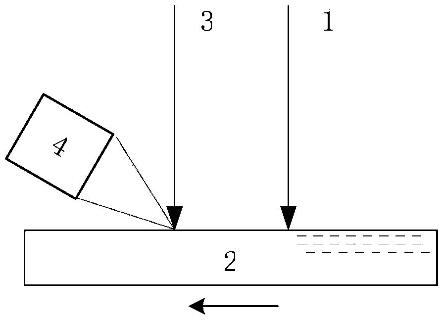
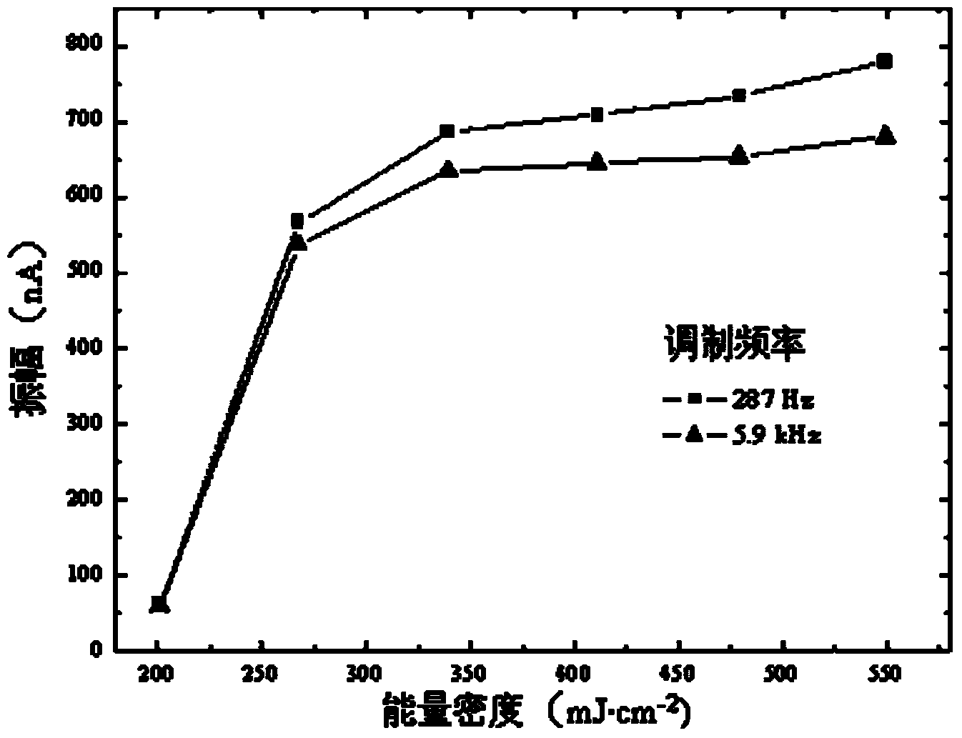
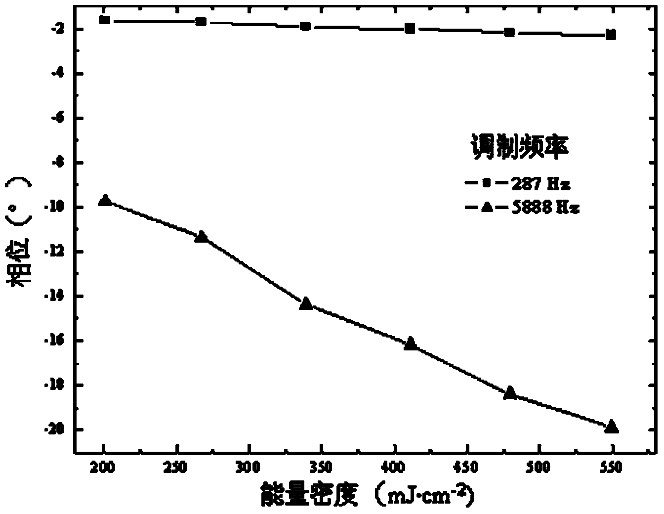
[0024] Such as figure 1 As shown, the annealing laser beam 1 output by the ArF excimer laser annealing device performs annealing treatment on the semiconductor material 2 . The excitation beam 3 in the optical detection system is output by a semiconductor laser with a center wavelength of 405nm (the photon energy generated by the excitation light is 3.06eV, which is greater than the intrinsic band gap of silicon 1.1eV), and its output power is 53mW, and passes through the function The signal generator performs periodic modulation; the photocarrier radiation signal is collected and detected by the infrared light detection device 4, which includes a long-wave pass filter for filtering the scattered light of the annealing laser beam and the excitation beam, and detects the photocarrier InP / InGaAs photomultiplier tube (PMT) detector for infrared r...


PUM


Abstract

The invention relates to a semiconductor silicon wafer laser annealing online detection method based on a photocarrier radio technology. The semiconductor silicon wafer laser annealing online detection method based on the photocarrier radio technology is characterized in that an optical detection system is added to a semiconductor material laser annealing device to achieve real-time online detection of the laser annealing; the optical detection system comprises an intensity periodically modulated stimulation light beam with photon energy larger than forbidden bandwidth of intrinsic semiconductor materials and a photocarrier infrared radiation signal collection device. According to the semiconductor silicon wafer laser annealing online detection method based on the photocarrier radio technology, laser annealing parameters are adjusted in real time due to comparing with photocarrier radiation signal data of reference samples, an expected annealing effect is achieved, and the annealing efficiency of the semiconductor materials is improved.

Description

technical field [0001] The invention relates to an on-line detection method for laser annealing of semiconductor materials, in particular to an on-line detection method for laser annealing of semiconductor silicon wafers based on photocarrier radiation technology. Background technique [0002] With the continuous reduction of the feature size of the semiconductor process, the ultra-shallow junction process has become a hot spot in the research of semiconductor process technology. In order to reduce the diffusion of impurities to meet the requirements of shallow junctions, it is necessary to use a new annealing technology to activate impurities and repair lattice damage. Compared with conventional thermal annealing, excimer laser annealing (S.Do, S.Kong, Y.Lee, J.Oh, J.Lee, M.Ju, S.Jeon and J.Ku, Ultra-shallow Junction Formation Using In the process of Plasma Doping and Excimer Laser Annealing for Nano-technology CMOS Applications, Journal of the Korean Physical Society.55, ...

Claims


Application Information

Patent Timeline
IPC IPC(8): H01L21/66H01L21/268
CPCH01L22/24
Inventor 李斌成王谦
Owner INST OF OPTICS & ELECTRONICS - CHINESE ACAD OF SCI
Why Eureka
Try Eureka