Thin film volume acoustic wave harmonic oscillator structure and manufacturing method thereof

A thin-film bulk acoustic wave and resonator technology, applied in the field of microelectronics, can solve the problems of large area of ​​silicon integrated circuits, reduce chip area, and insufficient reliability, so as to improve circuit performance, simplify manufacturing process, improve yield and stability Effect

Inactive Publication Date: 2014-04-16
江苏艾伦摩尔微电子科技有限公司
View PDF9 Cites 9 Cited by
  • Summary
  • Abstract
  • Description
  • Claims
  • Application Information

AI Technical Summary

Problems solved by technology

In 2008, the patent document WO 2008 / 101646 Al proposed a monolithic integration technology, which is to invert the FBAR, use a metal layer to support the electrical contact of the CMOS circuit, and form an air gap structure. This method can further reduce the chip area, but still Two sets of different processes are required to prepare FBAR and CMOS circuits separately, and this method uses a support structure, the reliability is not high enough, and the yield rate will be relatively low. Therefore, the existing integration technology requires a single silicon wafer area for the manufacture of FBAR. It is made on a silicon wafer, and the general area of ​​FBAR is 1~5*10 4 um 2 , which is too large and expensive for a silicon integrated circuit
In 2009, the patent document CN101630946A (a thin film bulk acoustic resonator and its preparation method) jointly applied by Zhejiang University and Tsinghua University proposed a method for preparing FBAR on the passivation layer, which further reduces the chip area, but requires Deposit a layer of Bragg acoustic wave reflection layer on the first layer and then make thin-film bulk acoustic resonator. Due to the deposition of Bragg emission layer, the thickness of each layer needs to be strictly controlled, and it is easy to fall off, and it is difficult to realize in the process.

Method used


Image

  • Thin film volume acoustic wave harmonic oscillator structure and manufacturing method thereof
  • Thin film volume acoustic wave harmonic oscillator structure and manufacturing method thereof
  • Thin film volume acoustic wave harmonic oscillator structure and manufacturing method thereof

Examples


Embodiment Construction

[0028] The present invention will be further described below in conjunction with the accompanying drawings.

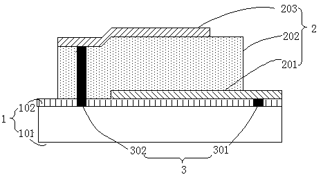
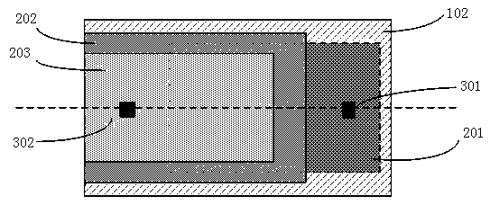
[0029] Such as figure 1 with figure 2 The thin film bulk acoustic resonator structure shown includes a substrate 1 and a piezoelectric stack 2 arranged on the surface of the substrate 1. The substrate 1 includes an integrated circuit chip 101 capable of processing the signal of the thin film bulk acoustic resonator and deposited and solidified on the integrated circuit. The polyimide layer 102 on the surface of the circuit chip 101, preferably, the thickness of the polyimide layer 102 is 1-70 μm, the integrated circuit chip 101 and the piezoelectric stack 2 are connected through the interconnection via hole 3, and the interconnection via hole 3 is filled with a conductive medium, and the conductive medium is tungsten. The integrated circuit of the integrated circuit chip 101 and the piezoelectric stack 2 realize the circuit connection through the interconnection hole...


PUM


Abstract

The invention discloses a thin film volume acoustic wave harmonic oscillator structure and a manufacturing method thereof. The method comprises the steps that a polyimide liquid coating is evenly coated on the surface of an integrated circuit chip directly in a spin mode, then a polyimide layer is formed between the high temperature of 170 DEG C and 250 DEG C in a solidifying mode, a piezoelectric stack structure is deposited on the surface of the polyimide layer, the polyimide layer is used as an acoustic reflecting layer, then interconnected through holes are formed, and the entire thin film volume acoustic wave harmonic oscillator structure and an integrated circuit of the integrated circuit chip are electrically connected through the interconnected through holes. According to the thin film volume acoustic wave harmonic oscillator structure and the manufacturing method thereof, the thin film volume acoustic wave harmonic oscillator structure comprises the integrated circuit chip, the polyimide layer and a piezoelectric stack, the structure is simple and reliable, integrated mechanical firmness is high, sensing is facilitated, and the thin film volume acoustic wave harmonica oscillator structure is applied to radio frequency or sensing systems and is suitable for various complex environments. The manufacturing method of the thin film volume acoustic wave harmonic oscillator structure is simple and quick, the production cycle is shortened, the production cost is lowered, and a good application prospect is achieved.

Description

technical field [0001] The invention relates to the technical field of microelectronics, in particular to a film bulk acoustic wave resonator structure and a preparation method thereof. Background technique [0002] In the field of wireless communication, high communication frequency, high transmission rate, high-intensity multiplexing and high integration have become the development trend, which puts forward higher requirements for the integration of components. At present, the integration of active devices into a chip is quite mature in semiconductor technology, but the research on the integration of passive devices is relatively small and immature, which seriously restricts the development of integration technology. Passive devices are mainly multiplexers, Filters, resonators, and matching LC networks, resonators can form multiplexers, filters, oscillators, etc. A wireless transceiver needs multiple resonators to form multiplexers, oscillators, and filters. Therefore, bas...

Claims


Application Information

Patent Timeline
Patent Type & Authority Applications(China)
IPC IPC(8): H03H9/17H03H3/02
Inventor 董树荣陈国豪郭维卞晓磊胡娜娜
Owner 江苏艾伦摩尔微电子科技有限公司
Why Eureka
Try Eureka