Monocrystalline silicon non-destructive surface nanometer machining method based on tribo-chemistry induction etching

A nano-fabrication, single crystal silicon technology, applied in the process of producing decorative surface effects, gaseous chemical plating, metal material coating process, etc., can solve the damage of single crystal silicon substrate, limit depth/height, resist etching It can avoid problems such as poor corrosion ability, etc., to achieve the effect of convenient scanning center, avoid friction loss, and simple film making process.

Active Publication Date: 2014-04-23
SOUTHWEST JIAOTONG UNIV
View PDF6 Cites 4 Cited by
  • Summary
  • Abstract
  • Description
  • Claims
  • Application Information

AI Technical Summary

Problems solved by technology

Common probe processing methods for single crystal silicon generally rely on anodic oxidation or friction. The influencing factors of anodic oxidation are complicated and have high requirements on the environment, so the processing cost is high; while the scanning probe used in the friction induction method is generally High-hardness diamond, in the process of processing, exerts pressure on

Method used


Image

  • Monocrystalline silicon non-destructive surface nanometer machining method based on tribo-chemistry induction etching
  • Monocrystalline silicon non-destructive surface nanometer machining method based on tribo-chemistry induction etching
  • Monocrystalline silicon non-destructive surface nanometer machining method based on tribo-chemistry induction etching

Examples


Embodiment 1

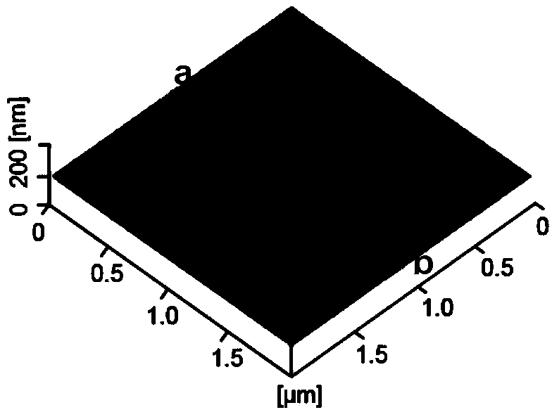
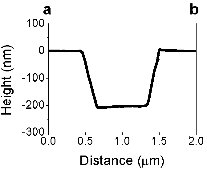
[0027] A non-damage nanofabrication method on the surface of single crystal silicon based on tribochemically induced etching, the specific operation steps are as follows:

[0028] A, the mass concentration is 98% H 2 SO 4 solution and 30% H 2 o 2 The solution is mixed according to the volume ratio of 7:3 to obtain a mixed solution; the mixed solution is heated to 90°C; then the single crystal silicon that has been passivated by the HF solution is placed in the mixed solution for 30 minutes to make SiO grow on the surface x thin layer; then there will be grown SiO x The thin layer of monocrystalline silicon is taken out and cleaned;

[0029] B. Install the silicon dioxide probe with a spherical tip on the scanning probe microscope, fix the single crystal silicon obtained in step A on the sample stage, start the scanning probe microscope, and control the probe with a contact pressure of 1GPa according to The surface scanning track of 2μm×2μm performs surface scanning on the...

Embodiment 2

[0033] A non-damage nanofabrication method on the surface of single crystal silicon based on tribochemically induced etching, the specific operation steps are as follows:

[0034] A, the mass concentration is 98% H 2 SO 4 solution and 30% H 2 o 2 The solution is mixed according to the volume ratio of 7:3 to obtain a mixed solution; the mixed solution is heated to 90°C; then the single crystal silicon that has been passivated by the HF solution is placed in the mixed solution for 30 minutes to make SiO grow on the surface x thin layer; then there will be grown SiO x The thin layer of monocrystalline silicon is taken out and cleaned;

[0035] B. Install the silicon dioxide probe with a spherical tip on the scanning probe microscope, fix the single crystal silicon obtained in step A on the sample stage, start the scanning probe microscope, and control the probe with a contact pressure of 1GPa according to The surface scanning track of 2μm×2μm performs surface scanning on the...

Embodiment 3

[0039] A non-damage nanofabrication method on the surface of single crystal silicon based on tribochemically induced etching, the specific operation steps are as follows:

[0040] A, the mass concentration is 98% H 2 SO 4 solution and 30% H 2 o 2 The solution is mixed according to the volume ratio of 7:2 to obtain a mixed solution; the mixed solution is heated to 80°C; then the single crystal silicon that has been passivated by the HF solution is placed in the mixed solution for 25 minutes, so that SiO can grow on the surface x thin layer; then there will be grown SiO x The thin layer of monocrystalline silicon is taken out and cleaned;

[0041] B. Install the silicon dioxide probe with a spherical tip on the scanning probe microscope, fix the single crystal silicon obtained in step A on the sample stage, start the scanning probe microscope, and control the probe with a contact pressure of 1GPa according to The surface scanning track of 2μm×2μm performs surface scanning o...


PUM


Abstract

The invention provides a monocrystalline silicon non-destructive surface nanometer machining method based on tribo-chemistry induction etching, which is mainly applied to machining a monocrystalline silicon surface nanometer structure. The monocrystalline silicon non-destructive surface nanometer machining method has the special operation steps: generating a SiOx thin layer on a monocrystalline silicon surface through a wet oxidation method; taking the monocrystalline silicon with the SiOx thin layer growing out, and washing and fixing the SiOx thin layer on a sample table; mounting a silicon dioxide spherical probe on a scanning probe microscope or multiple-point contact micro-nanometer machining equipment; starting the equipment; controlling the probe to scan the surface of a sample according to set parameters; and arranging the sample into a mixed solution of a KOH solution and isopropanol, so as to finish a machining process. A SiOx mask used in the method has the advantages of simplicity and easiness of manufacturing and low cost; a contact pressure in a probe scanning process is very low, so that the yielding of a monocrystalline silicon substrate is avoided, and the machined monocrystalline silicon nanometer structure is long in service life; the SiOx thin-layer mask obtained by the wet oxidation method has a good effect and the machining depth can be increased.

Description

technical field [0001] The invention relates to a nano-processing method for the surface of single crystal silicon. Background technique [0002] Nanotechnology has a profound impact on the development of modern manufacturing science and technology. As the basis for device miniaturization, micro-nano manufacturing technology has become an important direction for the development of the manufacturing industry, reflecting a country's high-tech development level to a certain extent. Nano-manufacturing science is the basis for supporting the application of nano-technology. With the development of device miniaturization, ultra-precision and microfabrication have become the key technologies of micro / nano electromechanical systems (MEMS / NEMS), [0003] Single crystal silicon is widely used in MEMS / NEMS because of its excellent mechanical and physical properties. Currently commonly used single crystal silicon processing methods face challenges such as low resolution, low efficiency...

Claims


Application Information

Patent Timeline
IPC IPC(8): B81C1/00
Inventor 钱林茂郭剑陈磊余丙军宋晨飞
Owner SOUTHWEST JIAOTONG UNIV
Why Eureka
Try Eureka