

Damage-free nanofabrication of single crystal silicon surface based on tribochemically induced etching
A nano-fabrication, single-crystal silicon technology, used in processes for producing decorative surface effects, gaseous chemical plating, metal material coating processes, etc., can solve the problem of poor etching resistance, limited depth/height, single crystal Silicon substrate damage and other problems, to achieve the effect of simple film forming process, avoiding friction loss, and convenient scanning center
- Summary
- Abstract
- Description
- Claims
- Application Information
AI Technical Summary
Problems solved by technology
Method used
Image

Examples
Embodiment 1
[0027] A non-damage nanofabrication method on the surface of single crystal silicon based on tribochemically induced etching, the specific operation steps are as follows:
[0028] A, the mass concentration is 98% H 2 SO 4 solution and 30% H 2 o 2 The solution is mixed according to the volume ratio of 7:3 to obtain a mixed solution; the mixed solution is heated to 90°C; then the single crystal silicon that has been passivated by the HF solution is placed in the mixed solution for 30 minutes to make SiO grow on the surface x thin layer; then there will be grown SiO x The thin layer of monocrystalline silicon is taken out and cleaned;
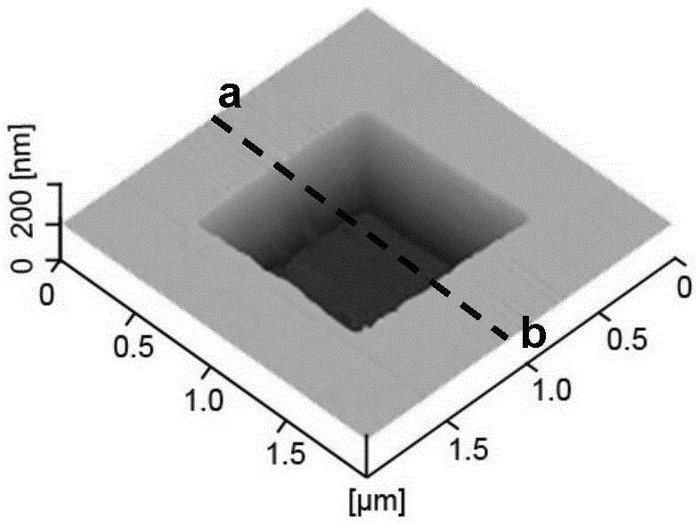
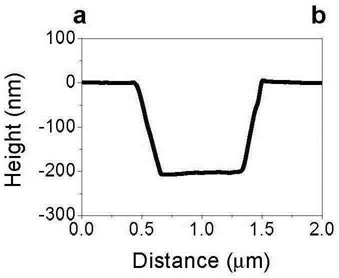
[0029] B. Install the silicon dioxide probe with a spherical tip on the scanning probe microscope, fix the single crystal silicon obtained in step A on the sample stage, start the scanning probe microscope, and control the probe with a contact pressure of 1GPa according to The surface scanning track of 2μm×2μm performs surface scanning on the...
Embodiment 2
[0033] A non-damage nanofabrication method on the surface of single crystal silicon based on tribochemically induced etching, the specific operation steps are as follows:
[0034] A, the mass concentration is 98% H 2 SO 4 solution and 30% H 2 o 2 The solution is mixed according to the volume ratio of 7:3 to obtain a mixed solution; the mixed solution is heated to 90°C; then the single crystal silicon that has been passivated by the HF solution is placed in the mixed solution for 30 minutes to make SiO grow on the surface x thin layer; then there will be grown SiO x The thin layer of monocrystalline silicon is taken out and cleaned;
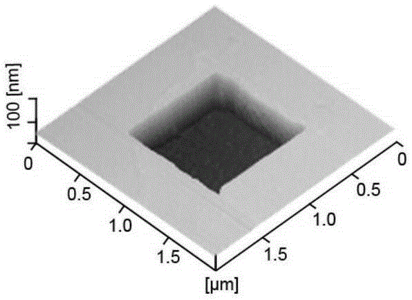
[0035] B. Install the silicon dioxide probe with a spherical tip on the scanning probe microscope, fix the single crystal silicon obtained in step A on the sample stage, start the scanning probe microscope, and control the probe with a contact pressure of 1GPa according to The surface scanning track of 2μm×2μm performs surface scanning on the...
Embodiment 3
[0039] A non-damage nanofabrication method on the surface of single crystal silicon based on tribochemically induced etching, the specific operation steps are as follows:
[0040] A, the mass concentration is 98% H 2 SO 4 solution and 30% H 2 o 2 The solution is mixed according to the volume ratio of 7:2 to obtain a mixed solution; the mixed solution is heated to 80°C; then the single crystal silicon that has been passivated by the HF solution is placed in the mixed solution for 25 minutes, so that SiO can grow on the surface x thin layer; then there will be grown SiO x The thin layer of monocrystalline silicon is taken out and cleaned;
[0041] B. Install the silicon dioxide probe with a spherical tip on the scanning probe microscope, fix the single crystal silicon obtained in step A on the sample stage, start the scanning probe microscope, and control the probe with a contact pressure of 1GPa according to The surface scanning track of 2μm×2μm performs surface scanning o...
PUM
 Abstract
Description
Claims
Application Information