Modularized array high-voltage LED chip and method for manufacturing modularized array high-voltage LED chip

An LED chip and array technology, applied in electrical components, electrical solid devices, circuits, etc., can solve the problems of packaging difficulties, rigid design methods, and chip packaging difficulties, so as to reduce manufacturing costs, and design methods are flexible and changeable. The effect of market demand

Inactive Publication Date: 2014-04-30
INST OF SEMICONDUCTORS - CHINESE ACAD OF SCI
View PDF5 Cites 8 Cited by
  • Summary
  • Abstract
  • Description
  • Claims
  • Application Information

AI Technical Summary

Problems solved by technology

like Figure 2A and Figure 2B All shown are the design methods of long strip structure. This kind of layout structure design is simple, the metal interconnection between each sub-unit is simple, and will not produce long interconnection leads, which will affect the reliability of the device; but once it is necessary to make For high-voltage LED chips with higher working voltage (such as 60V), more light-emitting subunits will be integrated inside the high-voltage LED chip. big difficulty
like Figure 2C and Figure 2D As shown, the high-voltage LED chip is designed as a square, which greatly improves the aspect ratio of the chip. The design method is relatively rigid, and it is impossible to produce 30V and 60V high-voltage chips at the same time

Method used


Image

  • Modularized array high-voltage LED chip and method for manufacturing modularized array high-voltage LED chip
  • Modularized array high-voltage LED chip and method for manufacturing modularized array high-voltage LED chip
  • Modularized array high-voltage LED chip and method for manufacturing modularized array high-voltage LED chip

Examples


Embodiment Construction

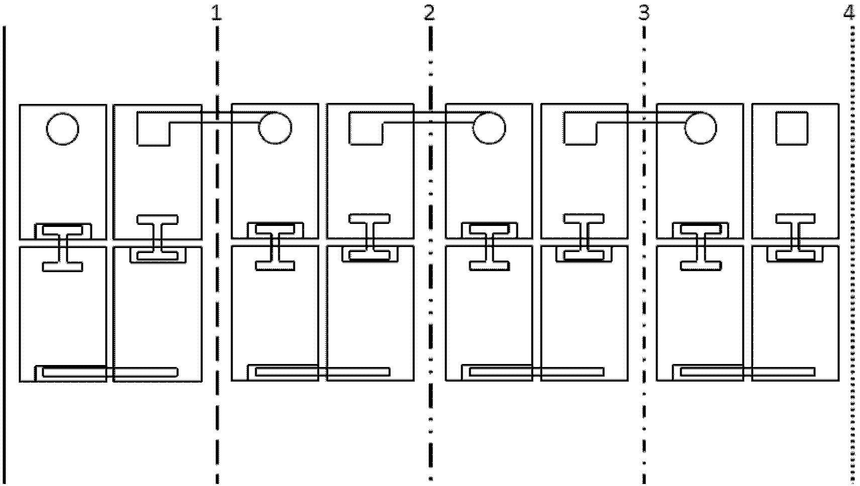
[0027] The LED chip structure includes a substrate, an N-type epitaxial layer, a quantum well light-emitting layer, a P-type epitaxial layer, interconnection leads, a P-type metal electrode and an N-type metal electrode. The substrate can be a homogeneous substrate or a heterogeneous substrate, either a planar substrate or a patterned substrate, and the thickness of the substrate is between 100 μm and 600 μm. Metal-organic chemical vapor deposition (MOCVD), hydride vapor phase epitaxy (HVPE) or molecular beam epitaxy (MBE) is used to grow epitaxial material structures on the substrate, and the thickness of the epitaxial structure ranges from 3 to 50 processes. First, a semiconductor material buffer layer is deposited on the substrate, and then an N-type doped material layer is grown; the quantum well light-emitting layer is grown on the N-type material layer; finally, a P-type doped layer is grown on the top of the epitaxial material structure. material layer.

[0028] Use pl...


PUM


Abstract

The invention discloses a modularized array high-voltage LED chip and a method for manufacturing the modularized array high-voltage LED chip. The modularized array high-voltage LED chip is composed of at least one unit module, wherein the unit module comprises at least one LED micro crystalline grain, all LED micro crystalline grains are insulated and isolated from one another and are integrated on a substrate, the LED micro crystalline grains of each unit module are connected in series in the mode that the LED micro crystalline grains are all connected with a lead, and all the unit modules are connected in series in the mode that the unit modules are connected with a lead. When the modularized array high-voltage LED chip is manufactured, an N type epitaxial layer, a quantum well luminescent layer and a P type epitaxial layer are grown on a substrate firstly, and a current barrier layer, an ITO transparent conducting layer and a metal electrode are manufactured on the P type epitaxial layer after a material surface, used for manufacturing an N electrode, of the N type epitaxial layer and insulating and isolating tracks between the LED micro crystalline grains are etched; then, cutting is conducted along the insulating and isolating tracks according to the laser scribing technology to obtain the modularized array high-voltage LED chip. According to the modularized array high-voltage LED chip and the method for manufacturing the modularized array high-voltage LED chip, both 30V array high-voltage chips and 60V array high-voltage chips can be obtained, manufacturing cost of the chips is reduced, and multiple chip machining alternatives are provided.

Description

technical field [0001] The invention belongs to the technical field of semiconductor lighting, and specifically relates to a modular array high-voltage LED chip and a manufacturing method thereof. Background technique [0002] As a new generation of green and environmentally friendly solid-state lighting sources, the luminous efficiency and reliability of GaN-based LEDs are constantly improving and improving. Compared with other traditional light sources, high-performance LEDs have significant advantages such as high photoelectric conversion efficiency, long life, low loss, and no pollution. They have been widely used in general lighting, traffic indicators, display backlights, and outdoor displays. Traditional LED device structure types include front-mount, vertical and flip-chip structures. The pn electrodes of the positive structure LED are located on the same side of the chip, and its disadvantages include poor heat dissipation and current crowding effect; the vertical ...

Claims


Application Information

Patent Timeline
Patent Type & Authority Applications(China)
IPC IPC(8): H01L27/15H01L33/00
Inventor 詹腾郭金霞田婷伊晓燕王莉李璟王国宏
Owner INST OF SEMICONDUCTORS - CHINESE ACAD OF SCI
Why Eureka
Try Eureka