
Radio-frequency power LDMOS device and manufacturing method thereof

A technology of radio frequency power and devices, which is applied in the field of radio frequency power LDMOS devices and its preparation, can solve the problems of reducing device power gain, etc., and achieve the effects of reducing parasitic gate-drain capacitance, good DC and RF characteristics, and improving DC characteristics

Inactive Publication Date: 2014-04-30
SHANGHAI LIANXING ELECTRONICS
View PDF0 Cites 3 Cited by
  • Summary
  • Abstract
  • Description
  • Claims
  • Application Information

AI Technical Summary

Problems solved by technology

Because the resistance and inductance of the source will generate negative feedback, reducing the power gain of the device

Method used


Image

  • Radio-frequency power LDMOS device and manufacturing method thereof
  • Radio-frequency power LDMOS device and manufacturing method thereof
  • Radio-frequency power LDMOS device and manufacturing method thereof

Examples


Embodiment 1

[0054] Channel region optimization design

[0055] 1. Gate oxide optimization design

[0056] LDMOS devices work in the saturation region. Transconductance is an important parameter to measure the amplification capability of the device. Its calculation formula is:

[0057] g m = ∂ I DS ∂ V GS | V BS , V DS Cons tan t = μ n W L C ox ( V GS - V T ) ...

Embodiment 2

[0073] Drift zone design optimization

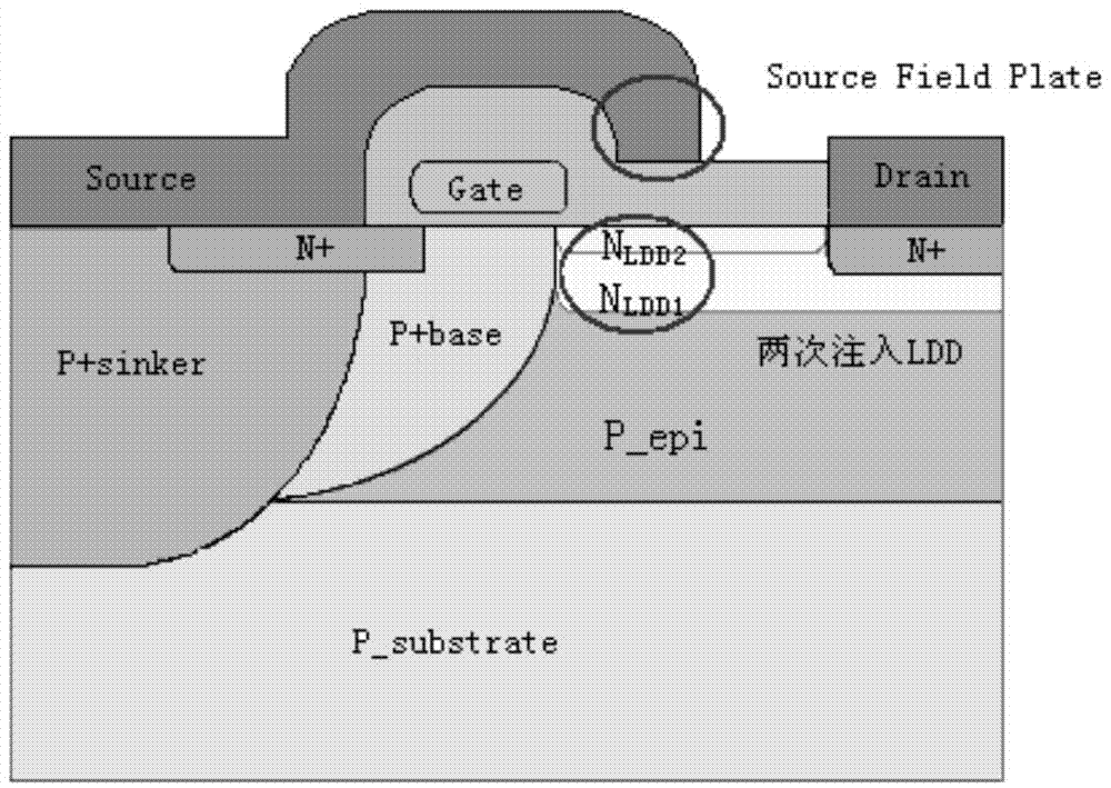
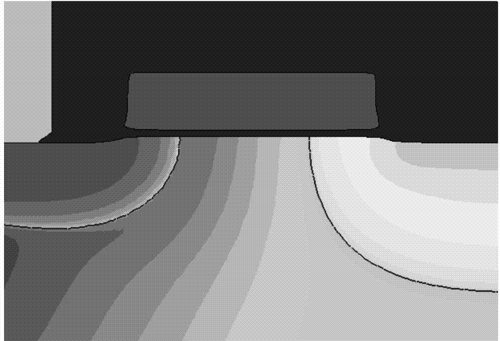
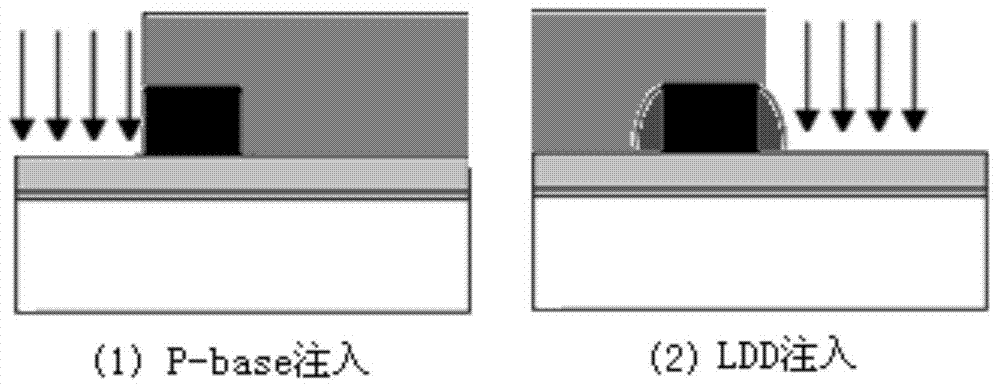
[0074] The research of the present invention finds that the requirements of the withstand voltage and on-resistance of the LDMOS device on the concentration and thickness of the drift region are contradictory. High breakdown voltage requires light doping, deep diffusion, and long drift region, while low on-resistance requires heavy doping, shallow diffusion, and short drift region. The LDMOS device in the present invention focuses on optimizing the doping implantation in the drift region on the premise that the design of the drift length can meet the requirement of the breakdown voltage. The drift region of the LDMOS of the present invention is implanted twice to form a deep junction LDD1 region and a heavily doped surface LDD2 region, and the same mask is used for the two implantations. The design process of the LDMOS drift region will be discussed in detail below.

[0075] 1. Design of drift zone length

[0076] The length of the dri...

Embodiment 3

[0087] SFP Field Board Optimization

[0088] The SFP plate is formed by elongating the source plate above the drift region to form a field plate when the metal is etched to form the source and drain metal contacts. When an SPF field plate is added above the drift region of the LDMOS device, since the field plate is connected to the source with a potential of 0, it can be found that the electric field lines in the drift region close to the drain region will shift towards the drain direction under the action of the field plate, so the SFP The field plate has the effect of optimizing the electric field in the drift region close to the gate region. Through the study of the drift region doping implantation in Example 2, it was found that when the LDD2 region was implanted with too high an impurity concentration, the breakdown occurred in the region of the drift region close to the gate, and the research of the present invention surprisingly found that, The SFP field plate can be u...


PUM

PropertyMeasurementUnit
Thicknessaaaaaaaaaa
Lengthaaaaaaaaaa

Abstract

The invention relates to a radio-frequency power LDMOS device and a manufacturing method of the radio-frequency power LDMOS device. The radio-frequency power LDMOS device comprises a source electrode, a grid electrode, a drain electrode, a silicon type substrate, a P-epi region, a P+sinker region, a P+base region, a gate oxide layer and an LDD region, wherein the LDD region is a drift region. Preferably, the edge of the gate oxide layer is provided with a beak structure and adopts a side wall process. On the condition of meeting the requirement of breakdown voltage, the radio-frequency power LDMOS device obviously reduces on resistance of the drift region and source leakage stray capacitance, evidently optimizes the characters of direct current and radio frequency, and has excellent performance and broad market prospects.

Description

technical field [0001] The invention relates to a radio frequency power device and a preparation method, more specifically a radio frequency power LDMOS device and a preparation method thereof. Background technique [0002] RF power devices are mainly used in RF power amplifiers of mobile communication system base stations in wireless communications. However, due to the lack of CMOS RF power performance, in the RF power semiconductor market, until the mid-1990s, RF power devices still used bipolar transistors or GaAs MOSFETs. Until the late 1990s, the emergence of silicon-based lateral diffusion transistor LDMOS changed this situation. Compared with bipolar transistors or GaAs MOSFETs, LDMOS devices have the advantages of high withstand voltage, large dynamic range of linear amplification at high frequencies, small distortion, high gain, high output power, and low cost, making them more than GaAs power devices. Gradually become the mainstream technology of RF power MOSFET....

Claims


Application Information

Patent Timeline
IPC IPC(8): H01L29/78H01L29/06H01L29/423H01L21/336
CPCH01L29/7816H01L29/0684H01L29/402H01L29/42364H01L29/66681
Inventor 杜寰朱喜福
Owner SHANGHAI LIANXING ELECTRONICS
Features
  • Generate Ideas
  • Intellectual Property
  • Life Sciences
  • Materials
  • Tech Scout
  • Unparalleled Data Quality
  • Higher Quality Content
  • 60% Fewer Hallucinations
Learn More