A kind of preparation method based on graphene field effect transistor

A technology of field-effect transistors and graphene, which is applied in the direction of transistors, semiconductor/solid-state device manufacturing, electrical components, etc., can solve problems such as expensive processing methods and unsatisfactory test results of graphene field-effect transistors, so as to save production costs, Effect of low power consumption and increased sensitivity

Active Publication Date: 2016-11-23
江苏好猫半导体有限公司
View PDF4 Cites 0 Cited by
  • Summary
  • Abstract
  • Description
  • Claims
  • Application Information

AI Technical Summary

Problems solved by technology

The thickness of graphene is too small, and the test results of graphene field effect transistors obtained under general micromachining conditions are not ideal, because the use of photoresist cannot be avoided in the process of pattern transfer, and the removal of photoresist is very important. Resist can change the properties of graphene. In summary, the processing of graphene-based micro-nano devices must rely on the method of electron beam exposure processing, which is relatively expensive.

Method used


Image

  • A kind of preparation method based on graphene field effect transistor
  • A kind of preparation method based on graphene field effect transistor
  • A kind of preparation method based on graphene field effect transistor

Examples


Embodiment Construction

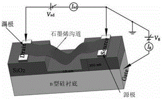
[0016] The present invention relates to graphene modification and a graphene-based compressive strain p-type field effect transistor manufacturing method, and the structure schematic diagram of the field effect transistor is as follows figure 1 shown, with a block doping concentration of 10 16 / cm 3 The n-type silicon wafer is used as the substrate, that is, the n-Si substrate, and the n-Si substrate is used as the back gate, and the back gate field effect transistor is prepared by a bottom-up processing method.

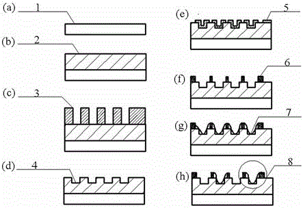
[0017] see figure 2 , figure 1 The fabrication steps of the graphene-based compressively strained P-type field effect transistor shown are as follows:

[0018] ① When the doping concentration is 10 16 / cm 3 Growth of 300 nm SiO by thermal dry oxidation on the surface of n-Si substrate 2 , control the temperature at 1000°C-1050°C for 20 minutes, such as figure 2 b.

[0019] ② To prevent SiO 2 If there are pollutants on the surface, first clean the SiO2 surf...


PUM

PropertyMeasurementUnit
widthaaaaaaaaaa
thicknessaaaaaaaaaa

Abstract

The invention relates to a graphene field effect transistor, in particular to a manufactured method of a transistor based on the graphene field effect. According to the method, metal gas source Ga ions are used for illuminating the surface of graphene, hole doping is carried out on the graphene, the Ga ions can lead pressure stress into the graphene, and the heat generated by illumination has an annealing function for the graphene. For the transistor based on the modified graphene field effect, the annealing function relieves the output nonlinearity of the field effect transistor, the led-in pressure stress opens the energy band structure of the graphene, the switch ratio of the graphene field effect transistor is improved, and the application of the field effect transistor in a logic circuit is promoted.

Description

technical field [0001] The invention relates to a graphene field effect transistor, in particular to a preparation method based on a graphene field effect transistor. Background technique [0002] Graphene is a carbon atom with sp 2 Hybridized orbitals form a hexagonal planar film with a honeycomb lattice. Due to the linear energy band structure dispersion near the Dirac point and the extremely high carrier mobility of both electrons and holes, graphene exhibits peculiar electronic properties. , such as the quantum spin Hall effect, based on the above reasons, graphene, as a next-generation semiconductor material, has attracted considerable attention. [0003] As far as the development of graphene-based micro-nano devices is concerned, it is important to precisely control the concentration and type of doped carriers. The doping methods that have been proposed so far mainly focus on the introduction of Ammonia (NH 3 ), synthesized doped graphene (X. R. Wang, X. L. Lin, L. ...

Claims


Application Information

Patent Timeline
Patent Type & Authority Patents(China)
IPC IPC(8): H01L21/335H01L21/3065
CPCH01L29/66045
Inventor 王权毛伟葛道晗张艳敏邵盈刘小颖
Owner 江苏好猫半导体有限公司
Why Eureka
Try Eureka