
IGBT device and manufacturing method thereof

A device, N-type technology, used in semiconductor/solid-state device manufacturing, semiconductor devices, electrical components, etc., can solve the problem of increasing IGBT device turn-off time, reducing forward voltage drop and turn-off time, and unsatisfactory IGBT device performance. and other problems, to achieve the effect of optimizing switching characteristics, increasing turn-off speed, and good turn-on and turn-off.

Active Publication Date: 2014-05-14
SHANGHAI LIANXING ELECTRONICS +2
View PDF3 Cites 3 Cited by
  • Summary
  • Abstract
  • Description
  • Claims
  • Application Information

AI Technical Summary

Problems solved by technology

Under blocking conditions, the electric field has a triangular distribution in the N-type base region, and its blocking voltage increases with the thickness of the N-type base region, and as the thickness of the N-type base region increases , its forward conduction voltage drop will also increase, and the turn-off time of the IGBT device will also increase, therefore, the performance of the conventional IGBT device is not ideal
[0004] In addition, there is an electric field blocking IGBT device. Compared with the conventional IGBT device, the electric field blocking IGBT device is provided with an N-type buffer layer between the collector region and the base region as an electric field blocking layer, which can Under the same blocking voltage, the thickness of the N-type base region can be reduced, so that the forward conduction voltage drop and turn-off time can be reduced, but the electric field blocking IGBT device is still not ideal.

Method used


Image

  • IGBT device and manufacturing method thereof
  • IGBT device and manufacturing method thereof
  • IGBT device and manufacturing method thereof

Examples


Embodiment Construction

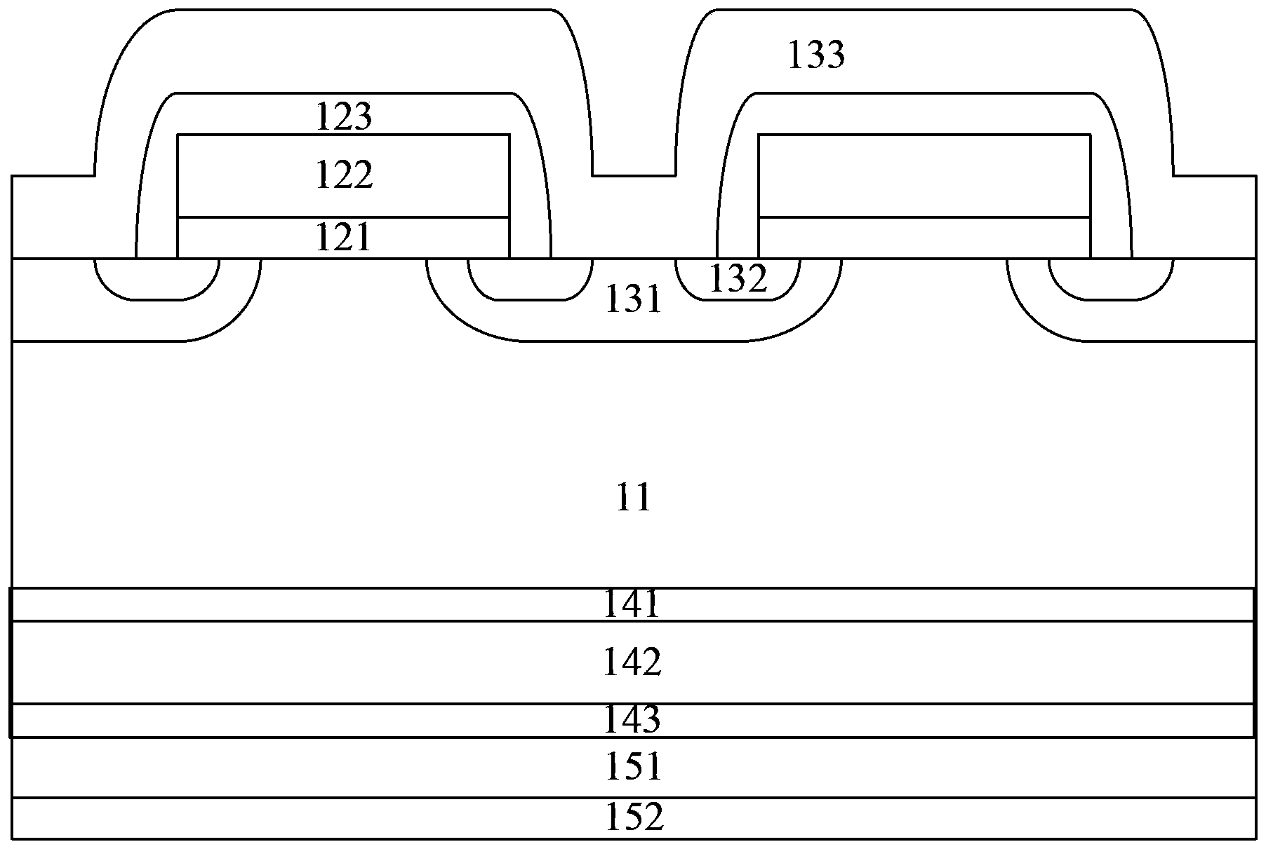
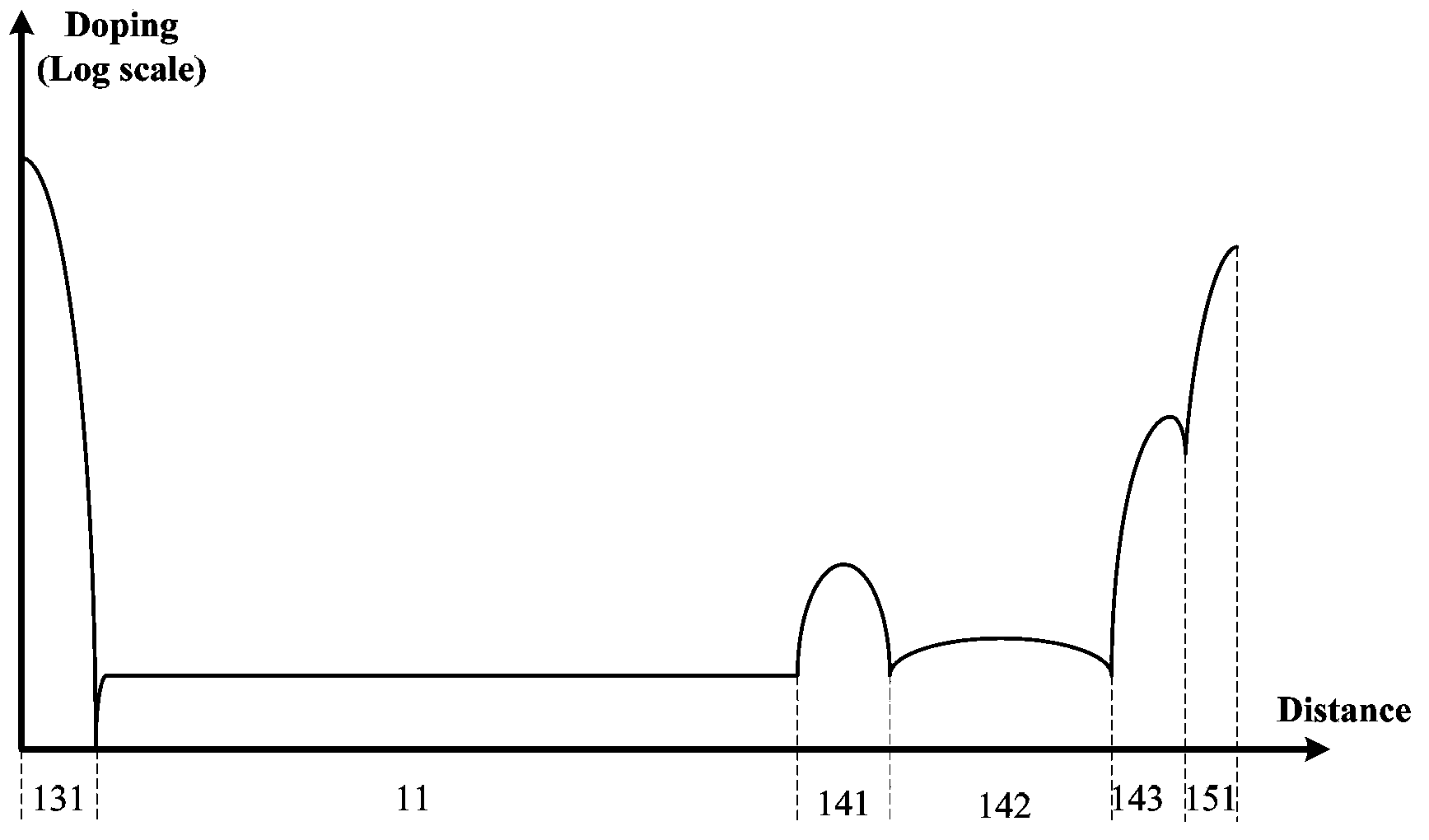
[0066] As mentioned in the background art, the performance of existing IGBT devices is not ideal. The inventors found that, for an electric field blocking IGBT device provided with an N-type buffer layer, in its blocking state, the electric field of the device is mainly distributed in the N-type base region, and between the N-type base region and the N-type At the junction of the N-type buffer layer, the electric field intensity distribution at the interface is determined by the doping concentration at the interface, and the voltage drop of the N-type buffer layer is determined by the thickness and doping concentration of the N-type buffer layer; in the N-type buffer layer and the collector structure At the collector region interface, the doping concentration of the collector region and the N-type buffer layer determines the injection efficiency of the device, and increasing the doping concentration of the N-type buffer layer will reduce the injection efficiency of the back col...


PUM


Abstract

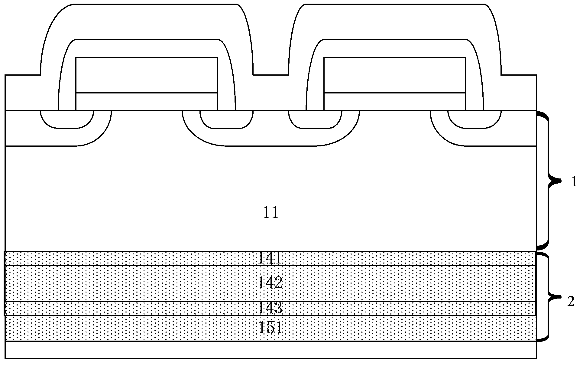
The embodiment of the invention discloses an IGBT device. A first N-type buffer layer, a second N-type buffer layer, and a third N-type buffer layer are successively disposed on the back surface of an N-type base region of the IGBT device. Impurities doped in the first N-type buffer layer are fifth main group element ions. The impurity concentration of the first N-type buffer layer is more than that of the N-type base region. Impurities doped in the second N-type buffer layer are sixth main group element ions. The impurity concentration of the second N-type buffer layer is more than that of the N-type base region but less than that of the first N-type buffer layer. Impurities doped in the third N-type buffer layer are fifth main group element ions. The impurity concentration of the third N-type buffer layer is more than that of the first N-type buffer layer. The three buffer layers are capable of respectively and independently optimizing correlative characteristics of the IGBT device in order to acquire a better on-gate and off-gate compromise curve. Further, the switching characteristic of the IGBT device is optimized such that the overall performance of the IGBT device is improved.

Description

technical field [0001] The invention relates to the technical field of semiconductor manufacturing, and more specifically, to an IGBT device and a manufacturing method thereof. Background technique [0002] Insulated Gate Bipolar Transistor (IGBT for short) is a composite fully-controlled voltage-driven power semiconductor device composed of a bipolar transistor (BJT) and an insulated gate field effect transistor (MOSFET), and has a MOSFET The advantages of the high input impedance of the device and the low conduction voltage drop of the power transistor (that is, the giant transistor, GTR for short), because the IGBT has the advantages of small driving power and low saturation voltage, the IGBT is currently used as a new type of power electronic device It is widely used in various fields. [0003] Existing conventional IGBT devices are fabricated using zone-melted single-crystal silicon substrates. Under blocking conditions, the electric field has a triangular distributio...

Claims


Application Information

Patent Timeline
Patent Type & Authority Applications(China)
IPC IPC(8): H01L29/739H01L29/06H01L21/331
CPCH01L29/0684H01L29/66333H01L29/7398
Inventor 胡爱斌朱阳军卢烁今王波吴振兴田晓丽赵佳陆江
Owner SHANGHAI LIANXING ELECTRONICS
Learn More