Phase change memory unit and method for manufacturing phase change memory unit

A phase change memory and phase change technology, applied in electrical components and other directions, can solve the problems of high operating power consumption, poor thermal stability, slow phase change speed, etc., to achieve the effects of ensuring reliability, prolonging life, and low power consumption

Inactive Publication Date: 2014-05-14
SHANGHAI INST OF MICROSYSTEM & INFORMATION TECH CHINESE ACAD OF SCI
View PDF5 Cites 26 Cited by
  • Summary
  • Abstract
  • Description
  • Claims
  • Application Information

AI Technical Summary

Problems solved by technology

[0005] In view of the above-mentioned shortcomings of the prior art, the object of the present invention is to provide a phase change memory unit and a preparation method thereof, which are used to solve the problems of slow phase transition speed, high operating power consumption, short life, thermal The problem of poor stability

Method used


Image

  • Phase change memory unit and method for manufacturing phase change memory unit
  • Phase change memory unit and method for manufacturing phase change memory unit
  • Phase change memory unit and method for manufacturing phase change memory unit

Examples


Embodiment 1

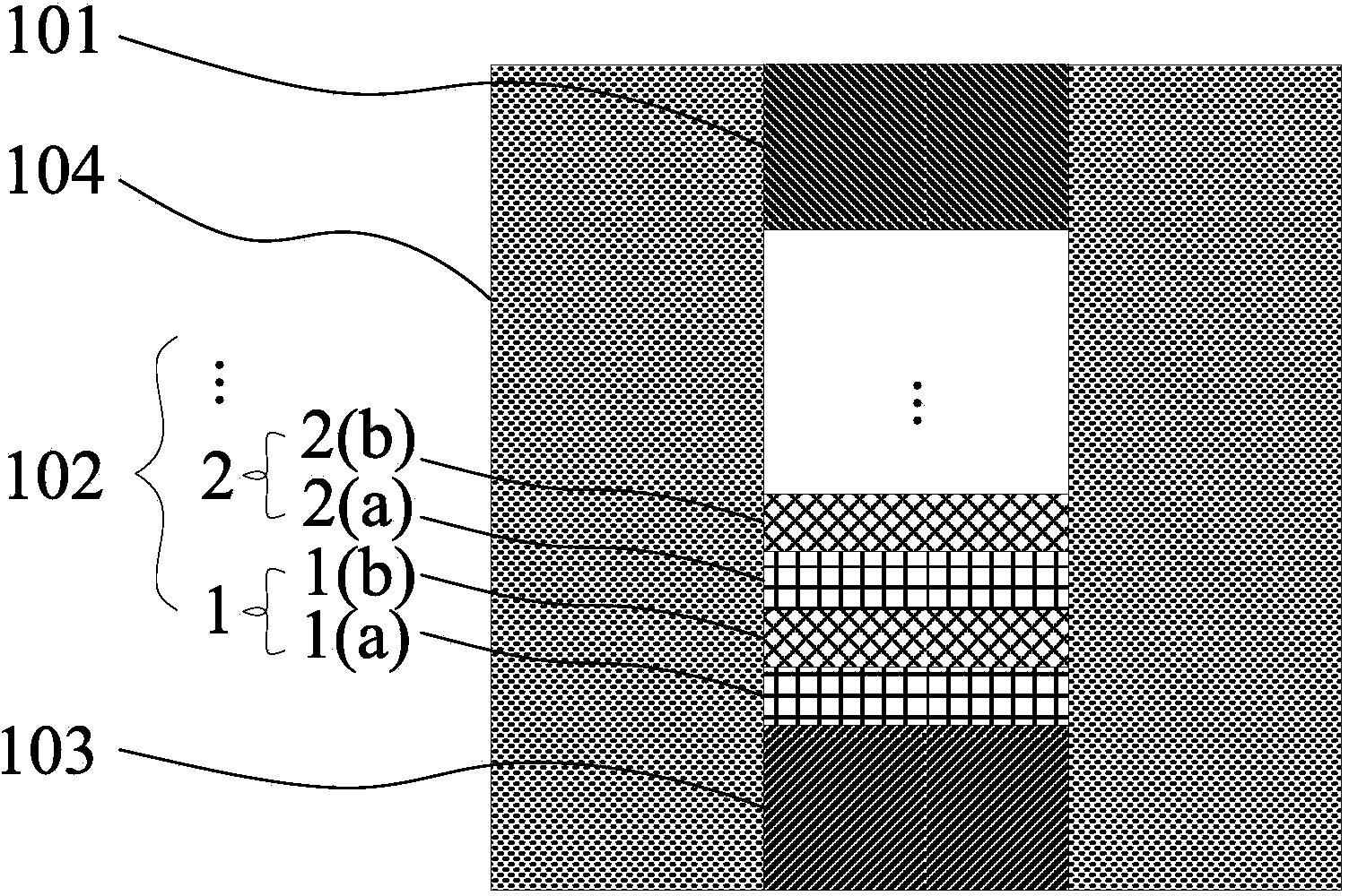
[0039] The present invention provides a phase change memory cell, such as figure 1 As shown, it includes a growth substrate, a lower electrode 103 , a dielectric cladding layer 104 , a phase change material layer (that is, a phase change superlattice film structure 102 ), and an upper electrode 101 .

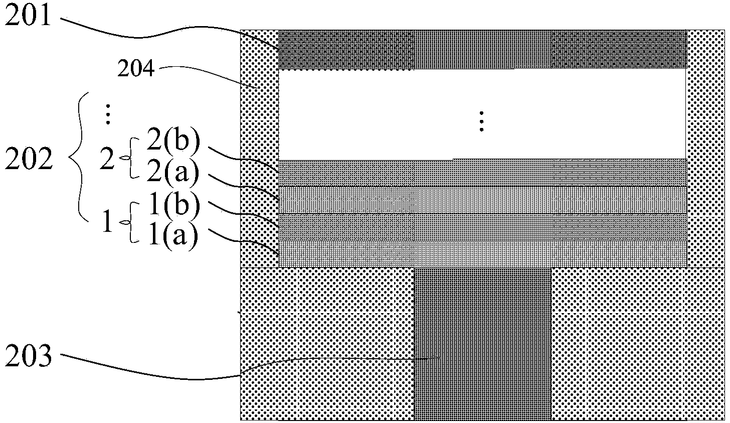
[0040]As an example, the phase-change memory cell may be a restricted structure or a T-shaped structure, such as figure 1 The structure of the restricted phase-change memory cell provided for the present invention; as figure 2 The structure of the T-type phase-change memory unit provided by the present invention.

[0041] The growth substrate can be a glass sheet or a silicon oxide substrate. In this embodiment, the growth substrate is a silicon oxide substrate.

[0042] The lower electrode 103 is fabricated in the growth substrate. The material of the lower electrode 103 can be Al, W, TiN or other conductive materials, and the thickness is in the range of 50-200 nm. In a sp...

Embodiment 2

[0046] The preparation method of the phase-change memory unit of the above-mentioned restricted structure comprises the following steps:

[0047] First, a growth substrate on which the lower electrode 103 is fabricated is provided.

[0048] Before performing subsequent processes, the growth substrate is cleaned to remove impurities such as organic matter, metal ions, and oxides on the surface of the growth substrate, which is beneficial to improving the stability of the device. The lower electrode 103 is a tungsten electrode with a thickness of 50-200 nm, and in a specific implementation process, it is 100 nm.

[0049] Then, a dielectric cladding layer 104 is deposited on the surface of the growth substrate.

[0050] The deposited dielectric cladding layer 104 may be SiO 2 or Si 3 N 4 . In this embodiment, the dielectric cladding layer is preferably Si 3 N 4 .

[0051] Next, the dielectric cladding layer 104 is etched by an exposure-etching process until a deposition h...

Embodiment 3

[0065] figure 2 The preparation method of the phase-change memory unit of T-type structure comprises the following steps:

[0066] Firstly, a growth substrate on which the lower electrode 203 is fabricated is provided.

[0067] Before performing subsequent processes, the growth substrate is cleaned to remove impurities such as organic matter, metal ions, and oxides on the surface of the growth substrate, which is beneficial to improving the stability of the device. The lower electrode 203 is a tungsten electrode with a thickness of 50-200 nm, and in a specific implementation process, it is 100 nm.

[0068] A phase-change material layer (phase-change superlattice film structure 202) and an upper electrode 201 are sequentially deposited in the deposition hole, and the phase-change material layer is composed of a single-layer phase-change material Sb x Te 1-x layer and monolayer compound Tiy Te 1-y A phase-change superlattice film structure formed by alternately vertically s...


PUM


Abstract

The invention provides a phase change memory unit and a method for manufacturing the phase change memory unit. A memory medium layer of the phase change memory unit is a superlattice thin film structure which is composed of an Sb[x]Te[1-x] layer and a Ti[y]Te[1-y] layer, and then a stable layered (Sb[x]Te[1-x])-(Ti[y]Te[1-y]) phase change material is obtained, wherein 0.4<=x<=0.8, 0.33<=y<=0.56, the thickness of the Sb[x]Te[1-x] layer is between 1 nm and 10 nm, and the thickness of the Ti[y]Te[1-y] layer is between 1 nm and 10 nm. The phase-change mechanism of the superlattice (Sb[x]Te[1-x])-(Ti[y]Te[1-y]) phase change material manufactured with the method is completely different from that of a traditional Ge-Sb-Te phase change material, and thus an obtained phase change memory device has the advantages of being lower in power consumption, higher in phase change speed, higher in retentivity, longer in service life and the like.

Description

technical field [0001] The invention relates to the field of semiconductor manufacturing materials, in particular to a phase-change memory unit and a preparation method thereof. Background technique [0002] Memory is an important part of the current semiconductor market and the cornerstone of information technology, playing an important role in both life and the national economy. With the rapid increase of the amount of information along with social development, the research and development of memory with high data storage density has become an important task for memory researchers. Among them, the phase-change memory unit is considered by the International Semiconductor Industry Association to be the most likely to be replaced due to its advantages such as high-speed reading, high erasable times, non-volatility, small component size, low power consumption, strong vibration resistance and radiation resistance. The current flash memory becomes the device that will become th...

Claims


Application Information

Patent Timeline
Patent Type & Authority Applications(China)
IPC IPC(8): H01L45/00
Inventor 饶峰丁科元夏梦娇宋志棠
Owner SHANGHAI INST OF MICROSYSTEM & INFORMATION TECH CHINESE ACAD OF SCI
Why Eureka
Try Eureka