Laser annealing device

A laser annealing and laser beam technology, applied in laser welding equipment, electrical components, circuits, etc., can solve the problems of low crystal absorption energy, inability to meet, low annealing efficiency, etc., to achieve good uniformity, high annealing efficiency, high The effect of the processing effect

Inactive Publication Date: 2014-05-28
SUZHOU DELPHI LASER
View PDF8 Cites 6 Cited by
  • Summary
  • Abstract
  • Description
  • Claims
  • Application Information

AI Technical Summary

Problems solved by technology

The traditional process is to bake and anneal in an annealing furnace of quartz glass. Due to the low melting point of the aluminum base, the temperature of the annealing furnace can only be less than 450 degrees, resulting in low energy absorption by the crystal, and the activation rate after annealing is only increased by 9-13%.
Its annealing efficiency is low and cannot meet the needs of market development

Method used


Image

  • Laser annealing device

Examples


Embodiment Construction

[0022] The present invention will be described in detail below in conjunction with specific embodiments shown in the accompanying drawings. However, these embodiments do not limit the present invention, and any structural, method, or functional changes made by those skilled in the art according to these embodiments are included in the protection scope of the present invention.

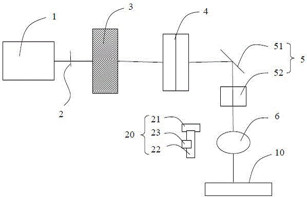
[0023] Please refer to figure 1 Shown is a schematic diagram of the overall structure of the laser annealing device of the present invention, including: a laser source 1, optical components, an image positioning system 20 and a control system. The laser beam emitted by the laser source 1 is adjusted and converted by the optical elements in the optical assembly to irradiate a flat-top spot with balanced energy. The flat-top spot has the advantages of high annealing efficiency and good uniformity, and at the same time improves the stability of the crystal arrangement. Activation rate, with higher proces...


PUM

PropertyMeasurementUnit
lengthaaaaaaaaaa
reflectanceaaaaaaaaaa

Abstract

The invention discloses a laser annealing device. The laser annealing device comprises a laser source which provides a laser beam, a beam expanding module which is located on an optical path of an output beam of the laser beam, a beam shaping module which is used for enabling a beam output by the beam shaping module to have uniform energy density, and a flat field focus lens which is located on an optical path of the output beam of the beam shaping module, and is used for focusing the beam output by the beam shaping module into flat topped light spots. According to the laser annealing device and a laser annealing method, which are provided by the invention, the optical components are used to carry out adjusting, and the flat topped light spots of uniform energy distribution are transmitted; the annealing efficiency is high; good uniformity is realized; the activation rate of crystal arrangement is improved; and effective processing is realized.

Description

technical field [0001] The invention relates to the technical field of laser annealing devices, in particular to a laser annealing device capable of improving the activation rate of crystal arrangement. Background technique [0002] With the rapid development of consumer electronics and home appliance industry, the high-voltage resistance of high-voltage integrated circuits is also gradually improving. High-voltage power integrated circuits commonly use BCD (Bipolar CMOS DMOS) technology. BCD is a manufacturing technology in the field of semiconductor power devices. It combines the high analog precision of Bipolar (insulated gate bipolar transistor, which is a composite full-control voltage-driven power semiconductor composed of bipolar triode insulated gate field effect transistor), the high integration of CMOS and the high power and high voltage characteristics. It was successfully developed by STMicroelectronics in 1986, which makes the device have the high transconducta...

Claims


Application Information

Patent Timeline
Patent Type & Authority Applications(China)
IPC IPC(8): H01L21/268B23K26/06
CPCH01L21/268H01L21/324
Inventor 赵裕兴韩伟汪昊徐海滨
Owner SUZHOU DELPHI LASER
Why Eureka
Try Eureka