
Photoelectric device with colloid NiO nanocrystalline film as hole transport layer and manufacturing method thereof

A hole transport layer, optoelectronic device technology, applied in semiconductor/solid-state device fabrication, organic light-emitting device fabrication/processing, organic semiconductor device fabrication/processing, etc. devices, etc., to achieve the effect of cost saving and simple preparation process

Active Publication Date: 2014-06-04
ZHEJIANG UNIV
View PDF4 Cites 26 Cited by
  • Summary
  • Abstract
  • Description
  • Claims
  • Application Information

AI Technical Summary

Problems solved by technology

[0007] The above-mentioned methods for preparing NiO hole transport layers have a common feature that the temperature in the preparation process is too high to prepare flexible photoelectric devices, which limits its further application.

Method used


Image

  • Photoelectric device with colloid NiO nanocrystalline film as hole transport layer and manufacturing method thereof
  • Photoelectric device with colloid NiO nanocrystalline film as hole transport layer and manufacturing method thereof
  • Photoelectric device with colloid NiO nanocrystalline film as hole transport layer and manufacturing method thereof

Examples


Embodiment 1

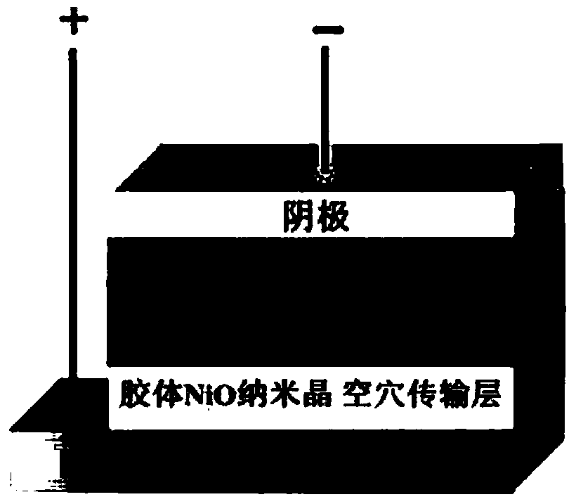
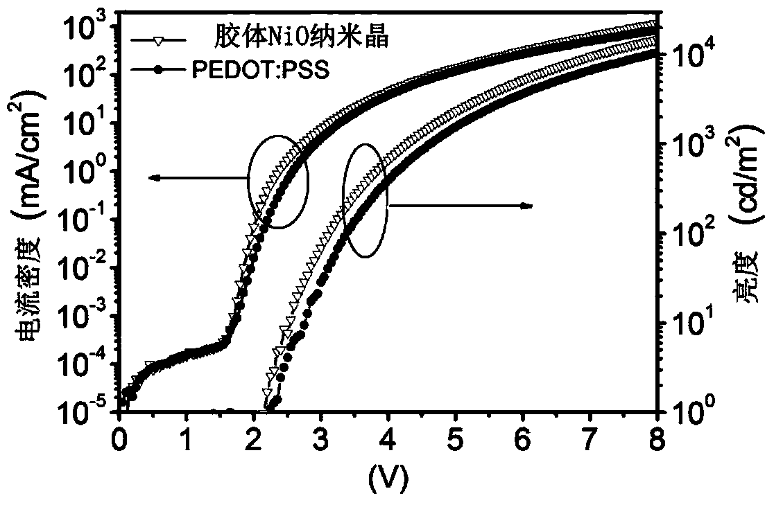
[0043] Example 1 Flexible organic LED device using colloidal NiO nanocrystalline thin film as hole transport layer

[0044] 1) Add 1mmol of nickel stearate, 0.2mmol of lithium stearate, and 6mmol of stearyl alcohol into 10ml of 1-octadecene, put it into a 50ml flask, heat up to 80°C under the protection of an inert gas, and pump Vacuum for 30 minutes; under the protection of inert gas, heat up to 280°C and keep warm for 120 minutes, cool to room temperature, add precipitant ethanol and centrifuge to obtain colloidal NiO nanocrystals;

[0045] 2) Mix 20 mg colloidal NiO nanocrystals with 0.5 ml chloroform to obtain a colloidal NiO nanocrystal solution, which is spin-coated on an ITO / PET substrate (commercially available) at a speed of 3000 Rpm / min to form a uniform and flat film, and then Annealed in air at 90°C for 120 minutes, and then treated with ozone for 10 minutes to obtain a colloidal NiO nanocrystalline film on the substrate;

[0046] 3) Mix 14mg MEH-PPV (manufacturer...

Embodiment 2

[0055] Example 2 Flexible organic LED device using colloidal NiO nanocrystalline thin film as hole transport layer

[0056] 1) Mix 15 mg of the colloidal NiO nanocrystals prepared in Example 1 with 0.5 ml of hexane to obtain a colloidal NiO nanocrystal solution, which is spin-coated on the ITO / PET flexible substrate at a speed of 1500 Rpm / min to form a uniform and flat The film was then annealed in air at 90°C for 140 minutes, and then treated with ozone for 10 minutes to obtain a colloidal NiO nanocrystalline film on the substrate;

[0057] 2) Mix 16mg MEH-PPV with 1ml dichlorobenzene to obtain a solution of MEH-PPV luminescent material, and spin-coat it on the colloidal NiO nanocrystalline film obtained in step 2) at a speed of 1500 Rpm / min to form a MEH-PPV luminescent layer ;

[0058] 3) ZnO thin film was prepared by thermal evaporation on the MEH-PPV light-emitting layer as an electron transport layer;

[0059] 4) Preparation of metal Al cathode on ZnO film.

[0060] T...

Embodiment 3

[0061] Example 3 Flexible organic solar cell using colloidal NiO nanocrystalline thin film as hole transport layer

[0062] 1) Mix 60 mg of colloidal NiO nanocrystals prepared in Example 1 with 1 ml of tetrachlorethylene to obtain a NiO nanocrystal solution, which is spin-coated on an ITO / PET substrate at a speed of 4000 Rpm / min to form a uniform and flat film, and then Annealed in air at 90°C for 120 minutes, and then treated with ozone for 10 minutes to obtain a colloidal NiO nanocrystalline film on the substrate;

[0063] 2) Add 20mg TQ1:PC 71 BM (manufacturer: Solenne) was mixed with 1ml of dichlorobenzene to obtain TQ1:PC 71 The solution of BM light-absorbing material was spin-coated on the colloidal NiO nanocrystalline film obtained in step 2) at a speed of 1200 Rpm / min to form TQ1:PC 71 BM light absorbing layer;

[0064] 3) In TQ1:PC 71 On the BM light absorbing layer, a ZnO thin film was prepared by thermal evaporation method as an electron transport layer;

[006...


PUM


Abstract

The invention discloses a photoelectric device with a colloid NiO nanocrystalline film as a hole transport layer. The photoelectric device is sequentially provided with an anode, the hole transport layer, an active layer, an electronic transport layer and a cathode from bottom to top. The hole transport layer is the colloid NiO nanocrystalline film. The invention further discloses a manufacturing method of the photoelectric device. The manufacturing technology is simple, saves cost and is particularly suitable for manufacturing the flexible photoelectric component. Manufactured colloid NiO nanocrystalline has the performance of solid nano NiO material and the characteristic of being processed by the adoption of a low-temperature solution technology, the film is higher in stability and working function, enables hole transport to be easier and not only can reduce interface resistance of the device, but also can obviously improve the efficiency of hole transport as the hole transport layer, so that the performance of the photoelectric device is improved.

Description

technical field [0001] The invention relates to the field of photoelectric devices, in particular to a photoelectric device using a colloidal NiO nanocrystal thin film as a hole transport layer and a preparation method thereof. Background technique [0002] At present, optoelectronic devices with layered thin-film structures have aroused great interest. A flexible device is formed on the substrate. [0003] Among the optoelectronic devices with layered thin film structures, the two most common types are LEDs and solar cells. In order to improve the device performance of LEDs and solar cells, electron or hole transport layers are often introduced between the electrodes and the active layer to improve the carrier transport efficiency. The material used as the hole transport layer is often required to have a high work function, especially in flexible devices, it must also meet the process requirements for easy low-temperature solution processing. NiO is a P-type semiconducto...

Claims


Application Information

Patent Timeline
Patent Type & Authority Applications(China)
IPC IPC(8): H01L33/14H01L51/42H01L31/0264H01L31/18H01L33/00H01L51/48
CPCY02E10/549H10K71/00H10K30/00H10K50/15H10K2102/311Y02P70/50
Inventor 金一政梁骁勇叶志镇
Owner ZHEJIANG UNIV
Learn More