Method for forming fine patterns of semiconductor device using directed self assembly process

A technology of directional self-assembly and fine patterning, which is applied in semiconductor/solid-state device manufacturing, microstructure technology, and photolithography on patterned surfaces, etc. It can solve the problems of forming slot defects, the whole process is intricate, hardened patterns are difficult to remove, etc. question

Inactive Publication Date: 2014-06-04
DONGJIN SEMICHEM CO LTD
View PDF0 Cites 14 Cited by
  • Summary
  • Abstract
  • Description
  • Claims
  • Application Information

AI Technical Summary

Problems solved by technology

Thus, the whole process is complicated
Since the hardened pattern (16a) is not easy to remove, it may cause defects when forming the slot

Method used


Image

  • Method for forming fine patterns of semiconductor device using directed self assembly process
  • Method for forming fine patterns of semiconductor device using directed self assembly process

Examples


example 1 and comparative example 1

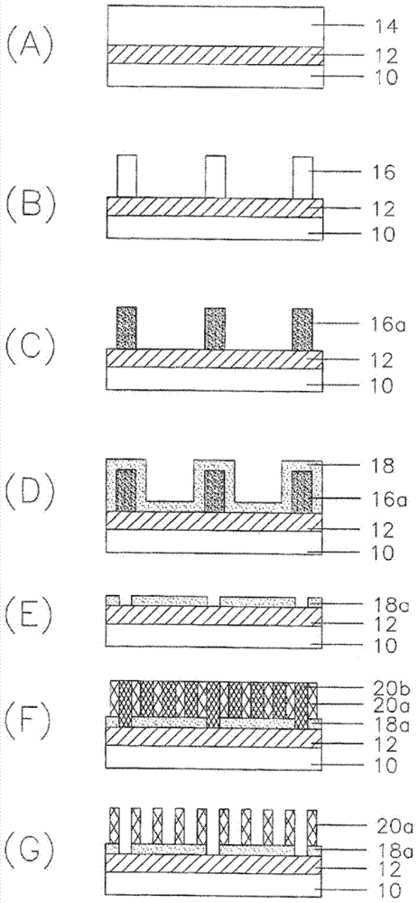
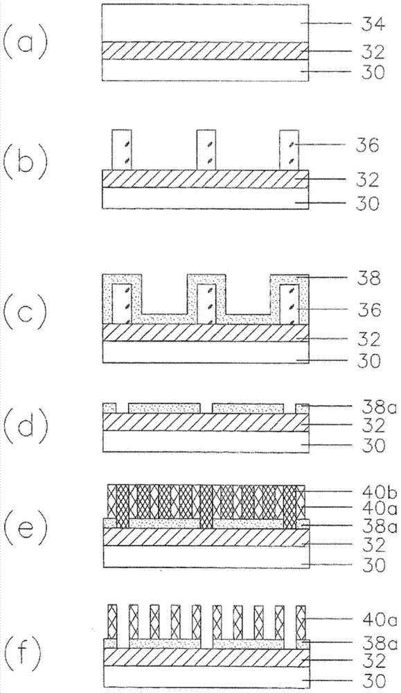
[0024] [Example 1 and Comparative Example 1] Formation of fine patterns of semiconductor devices and their evaluation

[0025] A 33 nm argon fluoride organic anti-reflection coating composition (DARC-A125, manufactured by Toshin Semicon Co., Ltd.) was coated on the silicon wafer and heated at 240° C. for 60 seconds. A photoresist composition (DHA-7079 (argon fluoride photoresist), manufactured by Toshin Semicon Co., Ltd.) was coated and soft-baked at 105°C for 60 seconds to form a Linewidth photoresist pattern. Next, the wafer was exposed to an argon fluoride photolithography machine with an aperture number of 0.85 (ASML1200, manufactured by ASML) and heated at 95° C. for 60 seconds to amplify acidic substances generated during exposure. The heated wafer was dipped in a negative developing solution (n-butyl acetate) for 60 seconds and developed to form a line and space pattern (guide pattern) with a line width of 70 nm. In Comparative Example 1, after exposing the photoresis...


PUM


Abstract

A method for forming fine patterns of a semiconductor device, which can form patterns having a size of pattern line width of 20nm or less without a bulk exposure and hardening process for a guide pattern, includes: an (a) step of forming a photoresist layer on a substrate having an organic anti-reflection layer; a (b) step of forming a guide pattern by exposing the photoresist layer and developing the exposed photoresist layer using a negative tone developer; (c) step of forming a self assembly conductive layer on the substrate having the guide pattern; a (d) step of forming the self assembly conductive layer by removing the guide pattern using the developer; an (e) step of coating a block copolymer as a directed self assembly (DSA) material on the substrate coated with the self assembly conductive layer from which the guide pattern is removed, and forming self-assembled patterns by heating the block copolymer at the glass transition temperature or higher; and a (f) step of forming the fine patterns by selectively etching a part having a low resistance against the etching (or having a high etching speed) among the self-assembled patterns using O2 plasma.

Description

technical field [0001] The present invention relates to a method for forming a fine pattern of a semiconductor device, and in particular to a method for forming a fine pattern of a semiconductor device capable of forming a pattern with a line width of 20 nanometers order by using directed self-assembly technology (lithography), without requiring a large number of guide patterns Exposure (bulk-exposure) and hardening. Background technique [0002] The downsizing and high integration of semiconductor devices require a technique for realizing fine patterns of semiconductor devices. Among the methods of forming a fine pattern of a semiconductor device, the most effective method is to use a fine photoresist pattern obtained through development of an exposure process and a new incremental processing technology. However, the development of the exposure process incurs a lot of investment costs and reduces the utilization of conventional existing processes. Therefore, research on n...

Claims


Application Information

Patent Timeline
Patent Type & Authority Applications(China)
IPC IPC(8): H01L21/027
CPCB81C2201/0149H01L21/3086B81C1/00031H01L21/0337H01L21/0271G03F7/0002H01L21/0274
Inventor 李正烈张有珍李载禹金宰贤
Owner DONGJIN SEMICHEM CO LTD
Why Eureka
Try Eureka