

Absorbing layer structure for non-refrigeration long-wave infrared detector
A technology of long-wave infrared and absorbing layers, which is applied in the direction of instruments, measuring devices, scientific instruments, etc., can solve the problems of process incompatibility, difficulty in using line array and area array detectors, short absorption band, etc., and achieve firm adhesion and low specific heat capacity , Strong corrosion resistance
- Summary
- Abstract
- Description
- Claims
- Application Information
AI Technical Summary
Problems solved by technology
Method used
Image

Examples
example 1
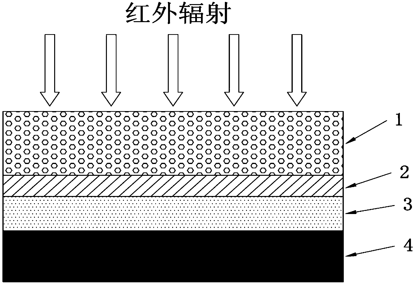
[0022] Based on Mn 1.56 co 0.96 Ni 0.48 o 4 In the heat-sensitive thin-film infrared detector, the long-wave infrared absorbing layer structure provided by this patent is adopted. Specifically, it is realized through the following steps.
[0023] (1) Mn 1.56 co 0.96 Ni 0.48 o 4 Preparation of thermosensitive film
[0024] 1) Preparation of Mn on amorphous alumina substrate by chemical solution method 1.56 co 0.96 Ni 0.48 o 4 Thin film with a thickness of about 3.5 μm.
[0025] (2) Etching to form electrode structure
[0026] 2) in Mn 1.56 co 0.96 Ni 0.48 o 4 The surface of the thin film is photolithographically patterned to form an etching mask.
[0027] 3) The photosensitive element of the detector is made by argon ion / HBr wet etching process, with an area of 0.09mm 2 . Float cleaning.
[0028] 4) Photolithographic patterning is carried out on the surface of the film, and 50nm of chromium and 200nm of gold are deposited as electrodes of the detector by ...
example 2
[0034] Based on Mn 1.56 co 0.96 Ni 0.48 o 4 In the heat-sensitive thin-film infrared detector, the long-wave infrared absorbing layer structure provided by this patent is adopted. Specifically, it is realized through the following steps.
[0035] (1) Mn 1.56 co 0.96 Ni 0.48 o 4 Preparation of thermosensitive film
[0036] 1) Preparation of Mn on amorphous alumina substrate by chemical solution method 1.56 co 0.96 Ni 0.48 o 4 Thin film with a thickness of about 3.5 μm.
[0037] (2) Etching to form electrode structure
[0038] 2) in Mn 1.56 co 0.96 Ni 0.48 o 4 The surface of the thin film is photolithographically patterned to form an etching mask.
[0039] 3) The photosensitive element of the detector is made by argon ion / HBr wet etching process, with an area of 0.09mm 2 . Float cleaning.
[0040] 4) Photolithographic patterning is carried out on the surface of the film, and 50nm of chromium and 200nm of gold are deposited as electrodes of the detector by ...
PUM
| Property | Measurement | Unit |
|---|---|---|
| Film thickness | aaaaa | aaaaa |
| Film thickness | aaaaa | aaaaa |
| Sheet resistance | aaaaa | aaaaa |
Abstract
Description
Claims
Application Information