Method for preparing nano-structured hard coating on surface of cemented carbide substrate

A technology of cemented carbide substrate and nanostructure, which is applied in metal material coating process, coating, ion implantation plating, etc., which can solve the problems of high cost of alloy target and difficulty in accurately controlling the content of Si element in the coating, etc.

Inactive Publication Date: 2014-07-02
XIAMEN UNIV
View PDF4 Cites 13 Cited by
  • Summary
  • Abstract
  • Description
  • Claims
  • Application Information

AI Technical Summary

Problems solved by technology

However, the cost of the alloy target is high, and it is difficult to accurately control the content of Si element in the coating

Method used


Image

  • Method for preparing nano-structured hard coating on surface of cemented carbide substrate
  • Method for preparing nano-structured hard coating on surface of cemented carbide substrate
  • Method for preparing nano-structured hard coating on surface of cemented carbide substrate

Examples


Embodiment 1

[0022] 1. Substrate pretreatment: (1) Grinding and polishing: Carry out sufficient rough grinding and fine grinding on the cemented carbide substrate on 600-mesh and 1200-mesh diamond grinding wheel discs respectively. Min, between coarse and fine grinding, the sample should be fully ultrasonically cleaned (ultrasonic cleaning time is 2min) and dried in an oven to remove wear debris and oil; after the sample is ground, use a W2.5 Diamond polishing powder is used for polishing, and the polishing time is 10 minutes. (2) Ultrasonic cleaning: Clean the polished substrate in the following order, ultrasonic cleaning with acetone for 5 minutes → ultrasonic cleaning with absolute ethanol for 5 minutes → drying for later use. (3) Ion source cleaning: Before sputtering deposition, the Hall ion source is used to clean the substrate, and the pressure of ion cleaning is 2×10 -2 Pa, substrate temperature 300°C, argon flux 10sccm, bias voltage negative 100V, cathode current voltage 29.5A, 1...

Embodiment 2

[0029] 1. Substrate pretreatment: (1) Grinding and polishing: Same as Example 1. (2) ultrasonic cleaning: with embodiment 1. (3) Ion source cleaning: Same as in Example 1.

[0030] 2. Pre-sputtering: same as embodiment 1.

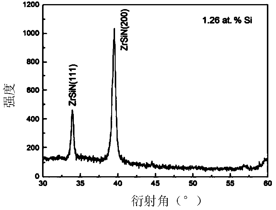
[0031] 3. Sputtering deposition: After the pre-sputtering, argon and nitrogen are introduced, the total flux is 60sccm, of which the nitrogen flow rate is 20%, the working pressure of the deposition is 0.3Pa, the DC power supply of the Zr target is 250W, Si The RF power of the target is 60W, the sputtering time is 90min, and the substrate temperature is 300°C. After the deposition is complete, the sample is taken out and stored in a desiccator, pending characterization and analysis. After the deposition is complete, the sample is taken out and stored in a desiccator, pending characterization and analysis.

[0032] image 3 It is the XRD spectrum of the coating, which shows that the prepared coating has a face-centered cubic structure. The method for m...

Embodiment 3

[0036] 1. Substrate pretreatment: (1) Grinding and polishing: Same as Example 1. (2) ultrasonic cleaning: with embodiment 1. (3) Ion source cleaning: Same as in Example 1.

[0037] 2. Pre-sputtering: same as embodiment 1.

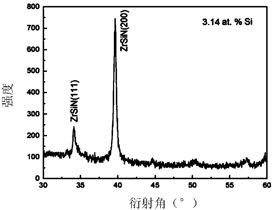
[0038] 3. Sputtering deposition: After the pre-sputtering, argon and nitrogen are introduced, the total flux is 60sccm, of which the nitrogen flow rate is 15%, the working pressure of the deposition is 0.4Pa, the DC power of the Zr target is 250W, Si The RF power of the target is 70W, the sputtering time is 90min, and the substrate temperature is 300°C. After the deposition is complete, the sample is taken out and stored in a desiccator, pending characterization and analysis. After the deposition is complete, the sample is taken out and stored in a desiccator, pending characterization and analysis.

[0039] Figure 4 It is the XRD spectrum of the coating, indicating that the prepared coating is a coating with a face-centered cubic structure. The coati...


PUM

PropertyMeasurementUnit
particle sizeaaaaaaaaaa
hardnessaaaaaaaaaa
particle sizeaaaaaaaaaa

Abstract

The invention discloses a method for preparing a nano-structured hard coating on the surface of a cemented carbide substrate. The cemented carbide substrate is subjected to grinding, polishing, ultrasonic cleaning, and ion source cleaning; pre-sputtering is performed; and sputtering deposition is implemented. By adopting a direct-current and radio-frequency reactive co-sputtering method, under the conditions of certain deposition pressure, temperature, nitrogen partial pressure and the like, a nano-structured hard coating is prepared on the surface of the substrate through controlling the Si target power. When the Si content of a ZrSiN coating is reduced, Si atoms exist in the coating in a form of substituting Zr atom, therefore, the ZrSiN coating with a low Si content is a solid liquid, and the cross section thereof is of a columnar structure. With the increasing of the Si content, the solid solubility of the ZrSiN coating is increased, so that the hardness of the ZrSiN coating is increased. When the Si content of the coating reaches a certain value, excess Si elements and N elements form amorphous Si3N4 at the grain boundary. With the further increasing of the Si content of the coating, a lot of amorphous Si3N4 is produced, and then the coating becomes an amorphous coating, and is of a non-columnar structure.

Description

technical field [0001] The invention relates to hard alloy surface treatment, in particular to a method for preparing a nanostructure hard coating on the surface of a hard alloy substrate. Background technique [0002] The study of hard materials is one of the important fields of material science research at present. With the rapid development of modern manufacturing and national defense industries, hard coating materials have been widely used in machinery manufacturing, automobile industry, textile industry, mold industry, aerospace and other fields. As a preparation method of material surface technology, coating technology can prepare various functional coatings. Combining the excellent properties of coatings and substrate materials, the performance of coating materials and substrate materials has been greatly improved, and the scope of application has been broadened. In this way, a very small amount of material can play the role of a large number of expensive overall mat...

Claims


Application Information

Patent Timeline
Patent Type & Authority Applications(China)
IPC IPC(8): C23C14/34C23C14/02C23C14/06
Inventor 王周成黄琳吴正涛
Owner XIAMEN UNIV
Why Eureka
Try Eureka