Etching composition containing copper metal layer used for display device and method of etching composition
A composition, copper metal technology, applied in the direction of instruments, optics, nonlinear optics, etc., can solve the problems of slow etching speed, lack of etching uniformity, etc., achieve uniform etching, excellent etching uniformity, and provide the effect of cost competitive advantage
- Summary
- Abstract
- Description
- Claims
- Application Information
AI Technical Summary
Problems solved by technology
Method used
Image
Examples
example 1
[0053] Example 1: Preparation of Etching Solution (1)
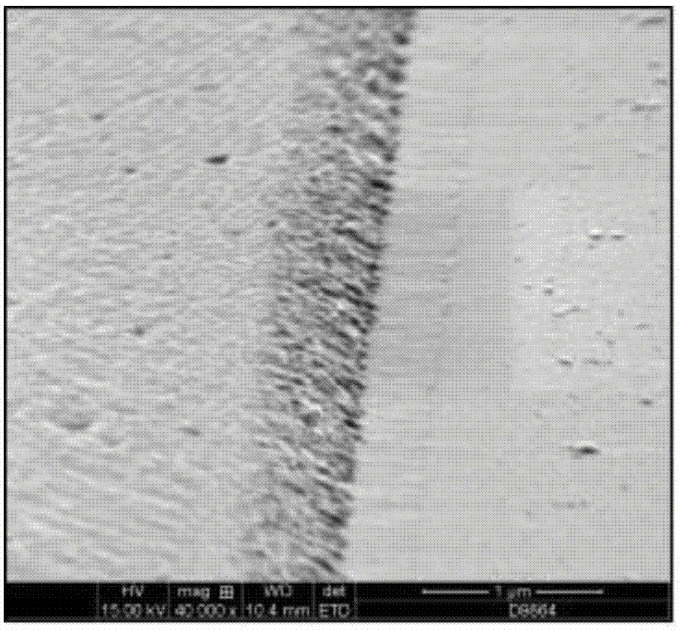
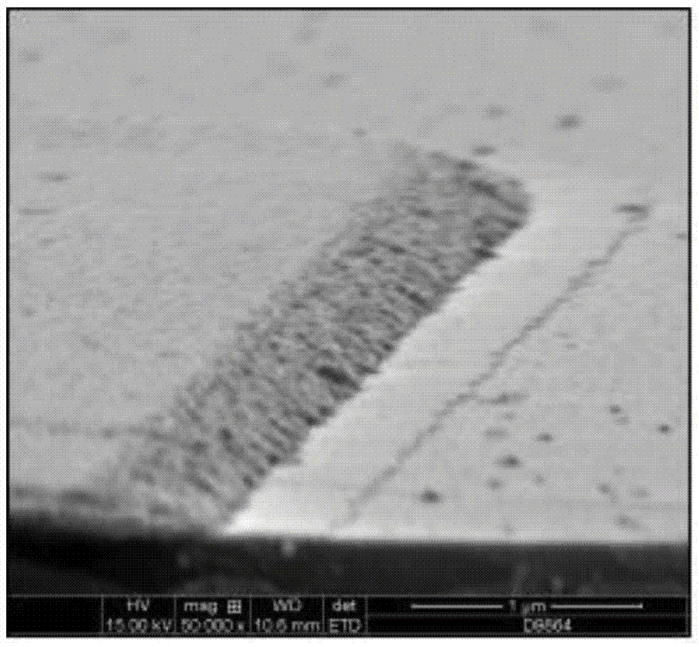
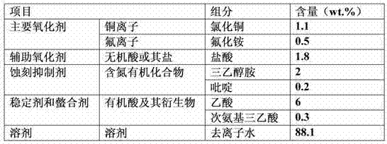
[0054]Prepare 2 L of an etching solution (comprising the following components) for the conductive metal layer in the LCD device. Etching was performed on the samples (20 mm × 20 mm) prepared by the above method with a spray etching device at a temperature of 30 °C under a pressure of 0.1 MPa for 35 s. ISJJX-Y-PP 020Y, IKEUCHI (2 L / min at 0.2 MPa) was used as one nozzle, and the spraying distance was 100 mm. The post-etch shape and surface state of the conductive metal layer in the LCD device were determined by using scanning electron microscopy (SEM).
[0055]
[0056]
[0057] The etching composition is used to etch a conductive metal layer in an LCD device. The exposed metal layer is selectively and clearly etched without damage to the photoresist layer. SEM was used to confirm a good taper angle (40° to 50°) of the etched copper. The etching rate of the copper layer constituting the conductive metal layer is 0...
example 2
[0059] Example 2: Preparation of Etching Solution (2)
[0060] Prepare 2 L of an etching solution (comprising the following components) for the conductive metal layer in the LCD device. Etching was performed on the samples (20 mm × 20 mm) prepared by the above method with a spray etching device at a temperature of 30 °C under a pressure of 0.1 MPa for 30 s. ISJJX-Y-PP 020Y, IKEUCHI (2 L / min at 0.2 MPa) was used as one nozzle, and the spraying distance was 100 mm. The post-etch shape and surface state of the conductive metal layer in the LCD device were determined by using scanning electron microscopy (SEM).
[0061]
[0062]
[0063] The etching composition is used to etch the conductive metal layer in the LCD device. The exposed metal layer is selectively and clearly etched without damage to the photoresist layer. A good taper angle (40° to 50°) of the etched copper was confirmed. The etching rate of the copper layer constituting the conductive metal layer is 0.30-0....
PUM
 Abstract
Description
Claims
Application Information
 - R&D Engineer
- R&D Manager
- IP Professional
- Industry Leading Data Capabilities
- Powerful AI technology
- Patent DNA Extraction
Browse by: Latest US Patents, China's latest patents, Technical Efficacy Thesaurus, Application Domain, Technology Topic, Popular Technical Reports.
© 2024 PatSnap. All rights reserved.Legal|Privacy policy|Modern Slavery Act Transparency Statement|Sitemap|About US| Contact US: help@patsnap.com


