Method and rolling cutter for manufacturing LED multi-chip package substrate

A LED substrate and multi-chip packaging technology, applied in semiconductor/solid-state device manufacturing, electrical components, circuits, etc., can solve the problems of complex tool routing, low processing efficiency, high cost, etc., and achieve simple process flow, less processing equipment, The effect of improving the utilization rate of materials

Active Publication Date: 2014-07-02
SOUTH CHINA UNIV OF TECH
View PDF4 Cites 0 Cited by
  • Summary
  • Abstract
  • Description
  • Claims
  • Application Information

AI Technical Summary

Problems solved by technology

[0003] However, since the integrated packaging substrate is a thin copper plate with a thickness of 1-1.5mm, the scale of the light-trapping structure belongs to the mesoscopic scale, and the distribution on the substrate is extremely dense. Therefore, it is necessary to process a high-density light-trapping microstructure on the surface of the substrate. The processing method is extremely difficult. Although special processing methods such as micro-milling and micro-EDM can process light-taking microstructures, the complex tool routing leads to low processing efficiency and high cost.

Method used


Image

  • Method and rolling cutter for manufacturing LED multi-chip package substrate
  • Method and rolling cutter for manufacturing LED multi-chip package substrate
  • Method and rolling cutter for manufacturing LED multi-chip package substrate

Examples


Embodiment 1

[0047] Taking the example of processing 1.5mm thick, taper hole side length 300×300um, taper hole depth 250um, taper hole spacing 350um, the substrate is copper plate, the process is as follows:

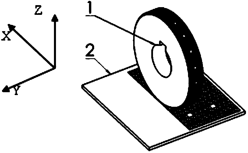
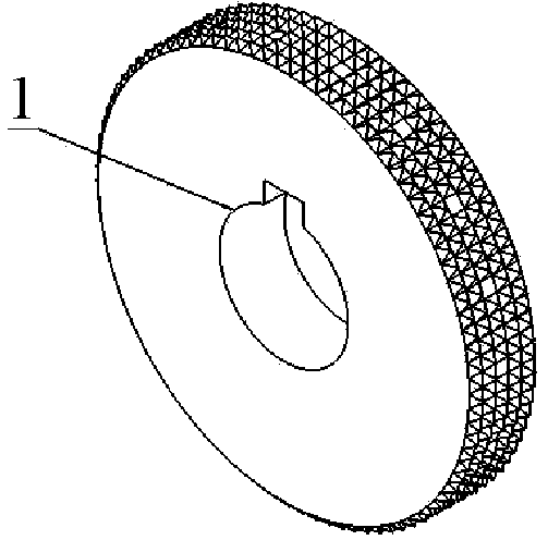
[0048](1) Design the rolling tool according to the structural size of the pre-prepared LED multi-chip integrated packaging substrate. The outer surface of the rolling tool has a five-row regular quadrangular pyramid structure, and this example adopts a regular quadrangular pyramid angle of 80°; this example uses a tool cone The tooth height is 400um, the outer diameter is 30mm, and the inner diameter is 10mm. The material is Cr12MoV. It is manufactured by precision grinding, and the surface roughness reaches Ra0.8. Remove a bevel tooth every 4 teeth on the middle row of the five-row bevel tooth structure of the pressing tool;

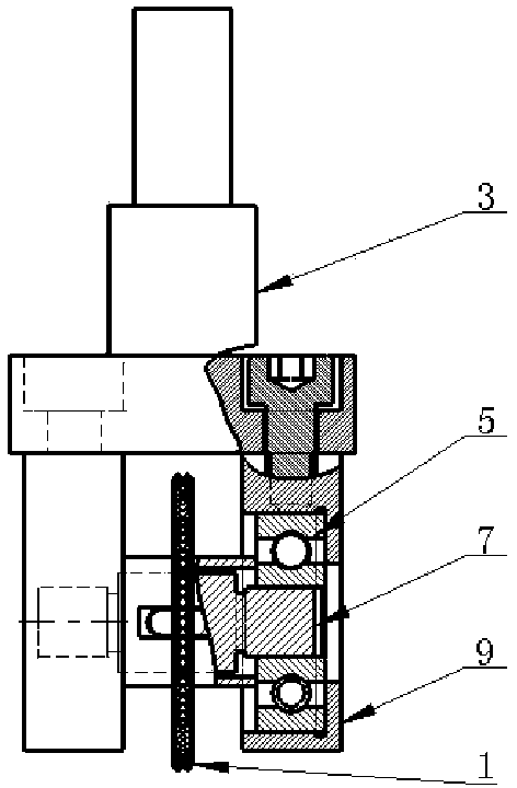
[0049] (2) Use the rolling fixture to fix the rolling tool on the main shaft of the ordinary vertical milling machine, and at the same time ensure that the si...


PUM


Abstract

The invention discloses a method and rolling cutter for manufacturing an LED multi-chip package substrate. The rolling cutter is fixed to a main shaft of a vertical milling machine, moving states of three shafts of the milling machine are respectively controlled, the pressing amount of the main shaft and the rolling speed of the rolling cutter are controlled, and accordingly the LED multi-chip integrated package substrate provided with an inverted right-square pyramid structure is obtained. The rolling cutter is manufactured in a precise cutting mode, the surface of the outer circle of the rolling cutter is provided with five columns of right-square pyramid structures, and the angle of each right-square pyramid ranges from 60 degrees to 100 degrees. The heights of conical teeth of the cutter range from 300 micrometers to 500 micrometers, the outer diameter of the cutter ranges from 30 mm to 50 mm, and the inner diameter of the cutter ranges from 10 mm to 15 mm. The method and rolling cutter can meet the manufacturing requirements of the LED multi-chip integrated package substrate provided with the inverted right-square pyramid light obtaining structure, substrate machining efficiency can be greatly improved, and compared with a traditional machining method, cost is lower and speed is higher.

Description

technical field [0001] The invention relates to the field of LED multi-chip integrated packaging and micro-manufacturing, in particular to a method for manufacturing an LED multi-chip packaging substrate and a rolling tool. Background technique [0002] Light-emitting diode (LED) has many advantages such as small size, long life, high electro-optical efficiency, environmental protection and energy saving, etc., and is considered to be the most promising new light source in the 21st century. If LED light source technology is applied to urban lighting, traffic lighting and residential lighting projects, it will make a huge contribution to the field of energy conservation and environmental protection. However, due to the defects of low luminous flux, low brightness and poor heat dissipation ability of LED single chip, it cannot be directly applied to general lighting. Scholars propose to use a patterned substrate to package and design the structure of the light source module. ...

Claims


Application Information

Patent Timeline
IPC IPC(8): H01L33/58H01L25/075H01L21/48B21D17/02
CPCB23P9/02H01L33/483H01L2933/0033
Inventor 简漳智万珍平李耀超李军辉
Owner SOUTH CHINA UNIV OF TECH
Why Eureka
Try Eureka