Growth method of compound semiconductor epitaxial layer on silicon substrate and device structure with epitaxial layer

A device structure and compound technology, which is applied in semiconductor devices, semiconductor/solid-state device manufacturing, electrical components, etc., can solve problems such as poor controllability, layer-to-layer cross-contamination, and increased manufacturing costs, and achieve cracks and dislocations. Effects of enhancing device performance and improving crystal quality

Active Publication Date: 2014-07-09
DEPOSITION EQUIP & APPL SHANGHAI LTD
View PDF4 Cites 39 Cited by
  • Summary
  • Abstract
  • Description
  • Claims
  • Application Information

AI Technical Summary

Problems solved by technology

Parameters such as crystal quality and component uniformity of each layer can only be known after the entire process is completed, so the metal-organic chemical vapor deposition method is complex and poorly controllable
Adding an aluminum nitride buffer layer to the production process of the epitaxial layer of semiconductor light-emitting diodes by metal-organic chemical vapor deposition method increases the difficulty of the process, easily brings cross-contamination between layers, and also significantly increases the manufacturing cost.
[0007] Although aluminum nitride can be deposited by other simple, low-cost methods, the crystal quality of aluminum nitride produced by such methods is inferior to that of aluminum nitride produced by metal organic chemical vapor deposition

Method used


Image

  • Growth method of compound semiconductor epitaxial layer on silicon substrate and device structure with epitaxial layer
  • Growth method of compound semiconductor epitaxial layer on silicon substrate and device structure with epitaxial layer
  • Growth method of compound semiconductor epitaxial layer on silicon substrate and device structure with epitaxial layer

Examples


Embodiment Construction

[0062] The present invention will be described in detail below in conjunction with specific embodiments shown in the accompanying drawings. However, these embodiments do not limit the present invention, and any structural, method, or functional changes made by those skilled in the art according to these embodiments are included in the protection scope of the present invention.

[0063] Furthermore, repeated reference numerals or designations may be used in different embodiments. These repetitions are only for the purpose of simply and clearly describing the present invention, and do not represent any relationship between the different embodiments and / or structures discussed.

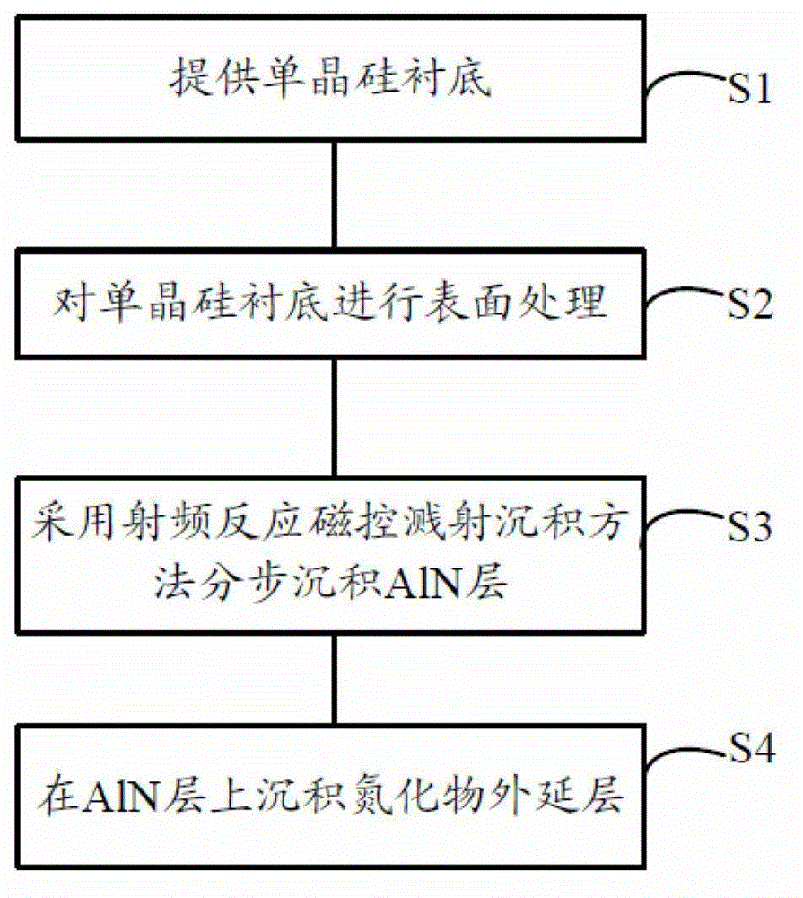
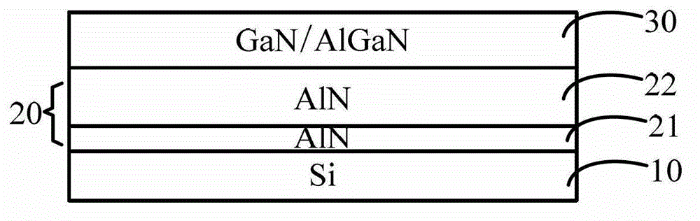
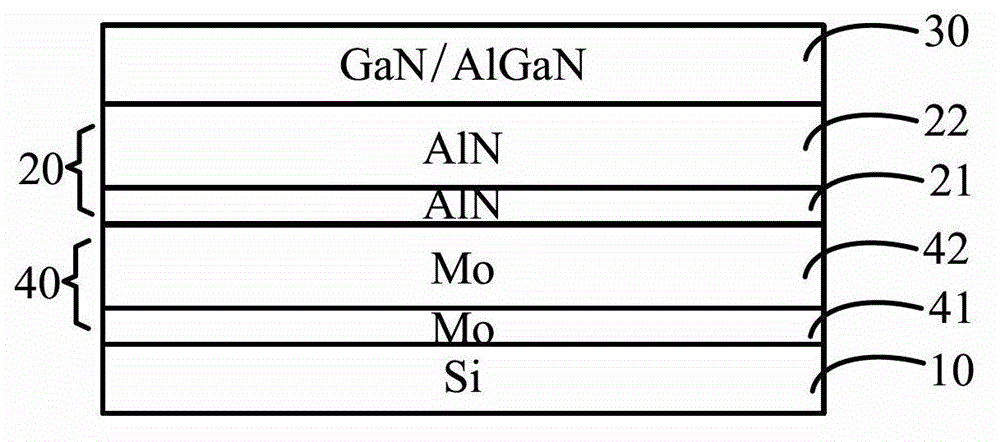
[0064] ginseng figure 1 Shown, the growth method of compound semiconductor epitaxial layer on a kind of silicon substrate of the present invention comprises:

[0065] S1. Provide a single crystal silicon substrate;

[0066] S2, performing surface treatment on the single crystal silicon substrate;

[...


PUM

PropertyMeasurementUnit
thicknessaaaaaaaaaa

Abstract

The invention discloses a growth method of a compound semiconductor epitaxial layer on a silicon substrate and a device structure with the epitaxial layer. The method comprises the steps of providing a single-crystal silicon substrate, carrying out surface processing on the single-crystal silicon substrate, depositing an AlN layer step by step through a radio frequency magnetron sputtering deposition method on the single-crystal silicon substrate, and depositing an AlN layer, or a GaN layer or an AlGaN layer on the AlN layer through an organometallic chemistry vapor deposition method or a hydride vapor phase epitaxy method. The AlN layer comprises an AlN nucleating layer used for controlling AlN crystal orientation and an AlN buffering layer used for controlling AlN crystal stress, and the AlN buffering layer is thicker than the AlN nucleating layer. The method effectively avoids the cracking and dislocation phenomenon caused by thermal mismatching and lattice mismatching, improves the crystal quality of the epitaxial layer, and enhances device performance.

Description

technical field [0001] The invention relates to the technical field of semiconductors, in particular to a method for growing a compound semiconductor epitaxial layer on a silicon substrate and a device structure thereof. Background technique [0002] Gallium nitride is considered to be the most important semiconductor material after silicon. GaN is a wide bandgap semiconductor material, its spectrum covers the entire visible light region, it can be made into blue and white light-emitting diodes for display, TV backlight and general lighting; it can be made into green / blue light-emitting diodes, Together with AlGaInP-based red light-emitting diodes, it is used for full-color display; it can also be made into ultraviolet lasers for data storage. In addition to excellent optical properties, electrical properties of gallium nitride are also excellent: high electron mobility (about 2000cm 2 / Vs), high electron velocity (2.5*10 7 cm / s), high critical electric field (3.5*10 6 V...

Claims


Application Information

Patent Timeline
Patent Type & Authority Applications(China)
IPC IPC(8): H01L33/32H01L21/20
CPCH01L21/02381H01L21/02458H01L21/0254H01L21/0262H01L21/02631
Inventor 马悦黄占超奚明
Owner DEPOSITION EQUIP & APPL SHANGHAI LTD
Why Eureka
Try Eureka