Method for preparing bipolar transistor of silicon carbide insulated gate of groove gate

A bipolar transistor and trench gate technology, applied in the field of microelectronics, can solve the problems of high preparation cost and difficult process, and achieve the effects of saving resources and energy, reducing preparation difficulty, and saving preparation cost and time.

Active Publication Date: 2014-07-16
XIDIAN UNIV
View PDF4 Cites 6 Cited by
  • Summary
  • Abstract
  • Description
  • Claims
  • Application Information

AI Technical Summary

Problems solved by technology

[0005] The purpose of the present invention is to propose a novel preparation method of trench-gate silicon carbide insulated gate bipolar transistors, so as

Method used


Image

  • Method for preparing bipolar transistor of silicon carbide insulated gate of groove gate
  • Method for preparing bipolar transistor of silicon carbide insulated gate of groove gate
  • Method for preparing bipolar transistor of silicon carbide insulated gate of groove gate

Examples


Embodiment 1

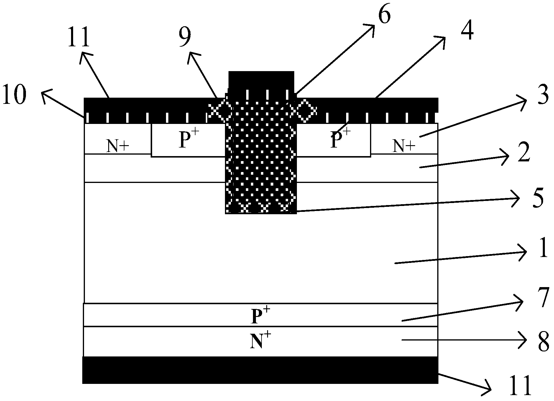
[0027] Example 1: Dislocations in the base plane are 10 4 / cm -3 , the substrate concentration is 3×10 14 cm -3 Trench-gate silicon carbide insulated gate bipolar transistors were fabricated on P-type SiC substrates with zero micropipe structure.

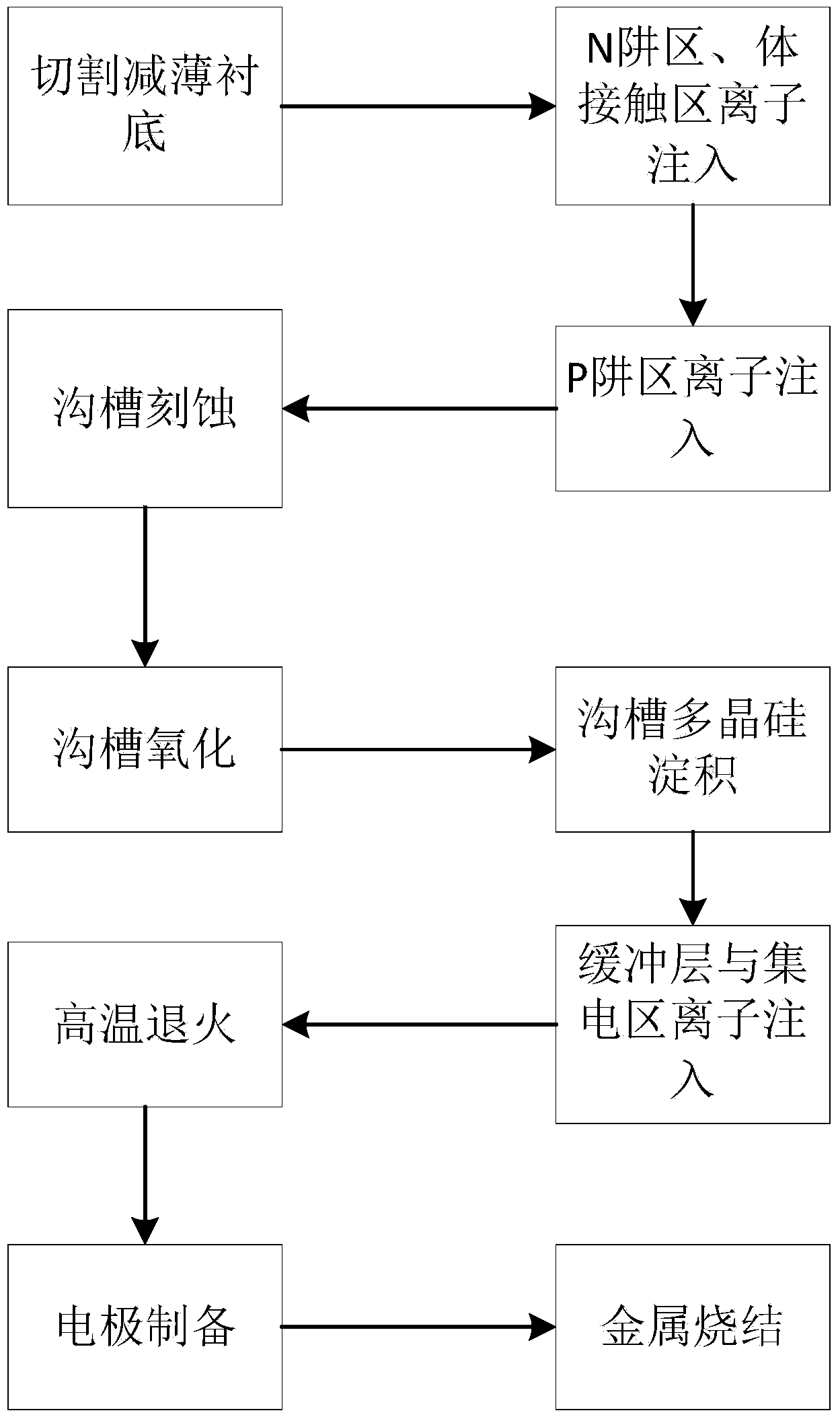
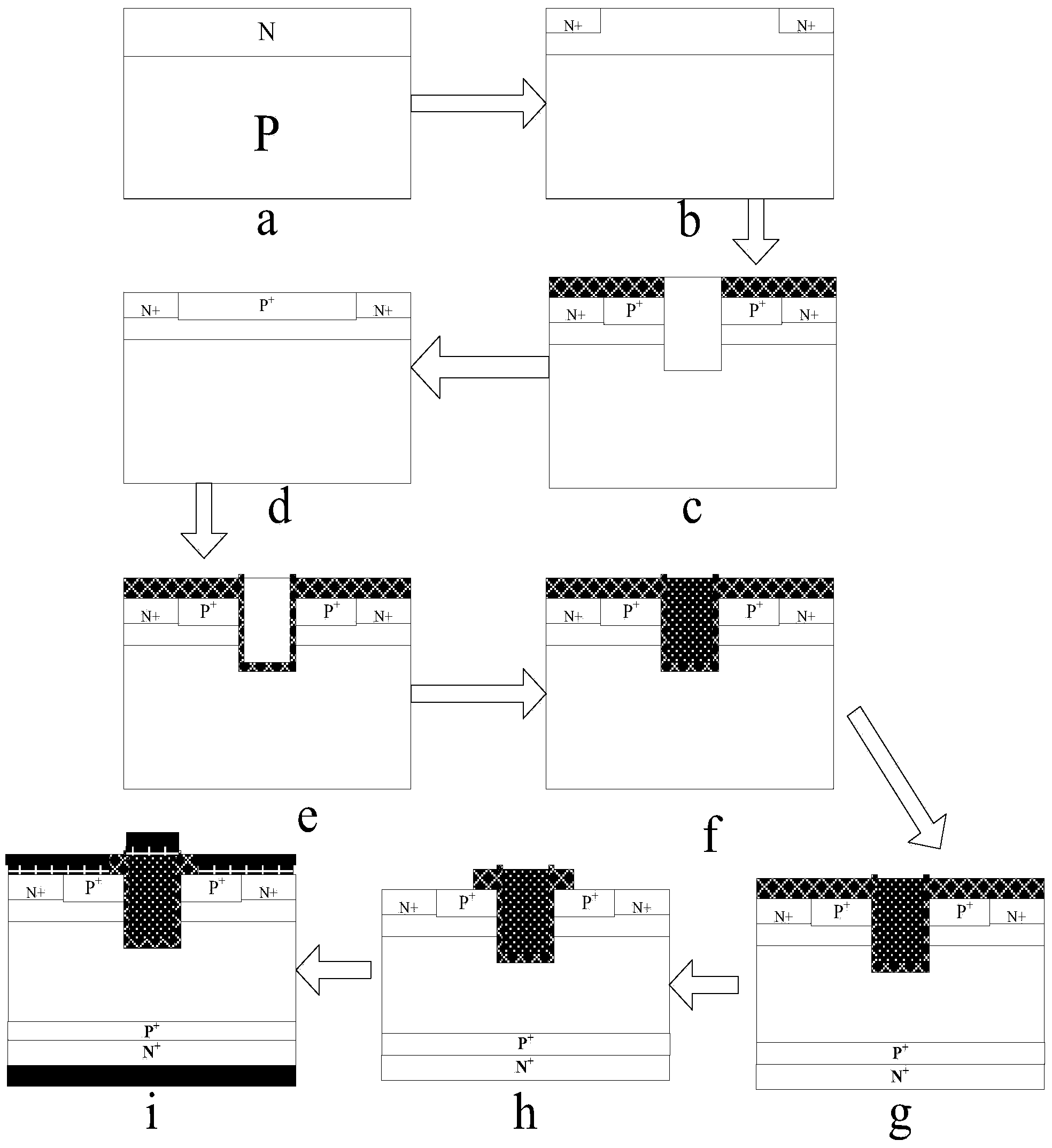
[0028] refer to figure 2 and image 3 , the implementation steps of this embodiment are as follows:

[0029] Step 1: Substrate processing.

[0030] The basal plane dislocation is chosen to be 10 4 / cm -3 , the substrate concentration is 3×10 14 cm -3 The P-type SiC substrate with zero micropipe structure is cut along the back surface of the P-type SiC substrate 1 to make it thinner to 100 μm; after polishing the cut surface, it is oxidized with wet oxygen at 950° C. for 20 minutes, and then the oxide layer is removed. Restore the cut surface structure and flatness.

[0031] Step 2: N well ion implantation.

[0032] (2.1) Deposit a layer of SiO with a thickness of 0.1 μm on the front side of the P-type SiC substrate afte...

Embodiment 2

[0059] Example 2: Dislocations in the base plane are 10 4 / cm -3 , the substrate concentration is 6×10 14 cm -3 Trench-gate silicon carbide insulated gate bipolar transistors were prepared on a micropipe-free P-type SiC substrate.

[0060] refer to figure 2 and image 3 , the implementation steps of this embodiment are as follows:

[0061] Step A: Substrate treatment.

[0062] This step is the same as Step 1 of Example 1.

[0063] Step B: N well ion implantation.

[0064] (b1) This step is the same as the step (2.1) of Example 1;

[0065] (b2) Perform two ion implantations on the window of the N well implantation region: at 650°C, first use 500Kev implantation energy, 4.5×10 12 cm -2 Implantation dose of nitrogen ion implantation, and then use the implantation energy of 350Kev, 1 × 10 12 cm -2 Implantation dose of the second nitrogen ion implantation, forming the N well region 2, such as image 3 Middle a.

[0066] Step C: Apply glue on the front side of the P-t...

Embodiment 3

[0081] Example 3: The dislocation in the base plane is 104 / cm -3 , the substrate concentration is 8×10 14 cm -3 Trench gate silicon carbide insulated gate bipolar transistors were prepared on the micropipe-free P-type SiC substrate.

[0082] refer to figure 2 and image 3 , the implementation steps of this embodiment are as follows:

[0083] The first step: substrate processing.

[0084] This step is the same as Step 1 of Example 1.

[0085] Step 2: Deposit a layer of Al with a thickness of 1.2 μm on the front of the above-treated P-type SiC substrate by low-pressure chemical vapor deposition as a barrier layer for nitrogen ion implantation, and coat the N well implantation area by photolithography Window: Perform two ion implantations on the window of the N well region at 650°C, that is, first use 700Kev implantation energy, 7.5×10 12 cm -2 Implantation dose of nitrogen ion implantation is performed once, and then with implantation energy of 450Kev, 4×10 12 cm -2 ...


PUM

PropertyMeasurementUnit
Thicknessaaaaaaaaaa
Thicknessaaaaaaaaaa
Thicknessaaaaaaaaaa

Abstract

The invention discloses a method for preparing a bipolar transistor of a silicon carbide insulated gate of a groove gate. The method mainly solves the problem that an existing bipolar transistor of a silicon carbide insulated gate is extremely high in preparing cost. The method comprises the steps that 1, a P-type carbide silicon substrate with good structural performance is selected, cutting and thinning are conducted on the back face of the substrate, and an oxide cutting face is polished; an N well region, an N+ body contact region and a P well region are sequentially formed on the front face of the substrate through ion implantation; 3, grooves are etched in the front face of the substrate, a groove gate oxide layer then grows, polycrystalline silicon deposition is conducted, and the grooves are filled with polycrystalline silicon; 4, ions on the back face of the substrate are implanted into a buffering layer and a collector region; 5, high-temperature annealing is conducted and implanted impurities are activated; 6, a device electrode is prepared. Compared with an existing method, a pressure-resistant layer with over-thick epitaxial is not needed, a large amount of production cost is reduced, the technical processes are simplified, and the method can be applied to the fields of inverters, switching mode power supplies and lighting circuits.

Description

technical field [0001] The invention belongs to the field of microelectronic technology, and relates to a method for preparing a semiconductor device, in particular to a trench gate structure SiC IGBT using a substrate as a voltage-resistant layer, which can be widely used in frequency converters, inverters, switching power supplies, and lighting circuits and motor fields. technical background [0002] Silicon carbide insulated gate bipolar transistor, or SiC IGBT, is a new type of high-voltage resistant device developed based on silicon carbide materials. At present, the mainstream solid-state device used in the field of power electronics is Si IGBT, and its turn-off voltage is 0.6-6.5kV. After 30 years of development, Si IGBT has reached the limit of performance and device structure. With the development of new applications such as electric vehicles, photovoltaic and wind energy green energy, and smart grids, a new leap in the performance of power electronic devices is re...

Claims


Application Information

Patent Timeline
IPC IPC(8): H01L21/331H01L21/265
CPCH01L29/66068
Inventor 郭辉翟华星张艺蒙宋庆文张玉明汤晓燕
Owner XIDIAN UNIV
Why Eureka
Try Eureka