

Method for improving N-typed DiMOSFET channel mobility based on N-typed nanometer thin layer
A mobility, N-type technology, applied in the field of microelectronics, can solve the problems of reduced gate oxide reliability, affected device performance, rough contact interface, etc., to reduce trap charges, increase mobility, and reduce interface roughness. Effect
- Summary
- Abstract
- Description
- Claims
- Application Information
AI Technical Summary
Problems solved by technology
Method used
Image

Examples
Embodiment 1
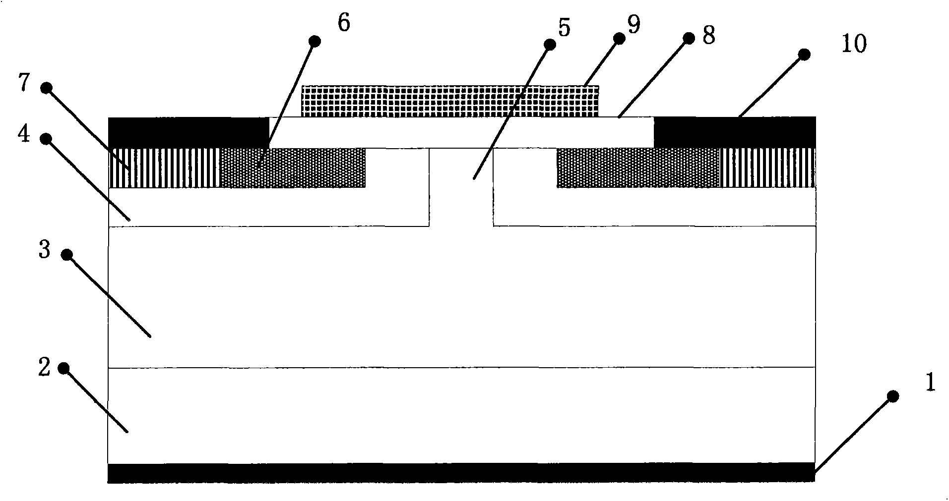
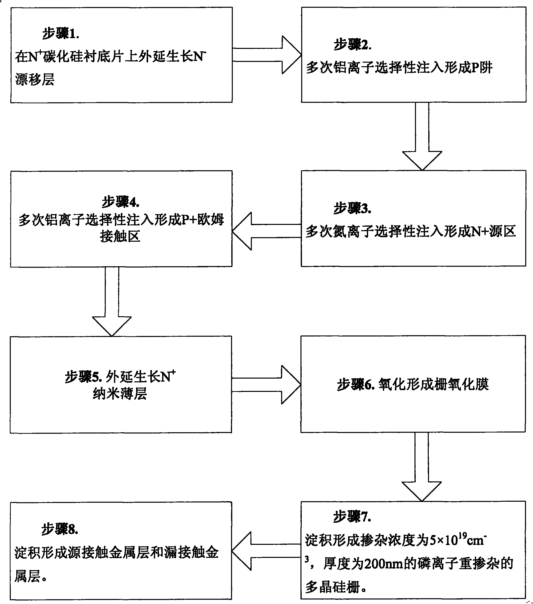
[0036] Step 1. In N + Epitaxial growth of N on SiC substrate - Drift layer.
[0037] to N + The silicon carbide substrate 2 was cleaned by RCA cleaning standard, and then epitaxially grown on the surface of the substrate with a thickness of 8 μm and a nitrogen ion doping concentration of 1×10 15 cm -3 N - Drift layer 3, such as figure 2 In step 1, the process conditions are as follows: the epitaxy temperature is 1570° C., the pressure is 100 mbar, the reaction gas is silane and propane, the carrier gas is pure hydrogen, and the impurity source is liquid nitrogen.
[0038] Step 2. Multiple times of selective implantation of aluminum ions to form a P well.
[0039] (2.1) Deposit a layer of SiO with a thickness of 0.2 μm on the front side of the silicon carbide wafer by low-pressure hot-wall chemical vapor deposition 2 layer, and then deposit Al with a thickness of 1 μm as a barrier layer for the ion implantation of the P well 4, and form the P well implantation region by...
PUM
| Property | Measurement | Unit |
|---|---|---|
| Thickness | aaaaa | aaaaa |
Abstract
Description
Claims
Application Information