Flexible and efficient crystalline silicon solar cell and manufacturing method thereof
A technology for solar cells and manufacturing methods, applied in the direction of final product manufacturing, sustainable manufacturing/processing, circuits, etc., can solve the problems of long and complex process, high manufacturing cost, and high technical route difficulty, achieve wide application, easy to low cost and high cost. The effect of large-scale industrialization and excellent photoelectric performance
- Summary
- Abstract
- Description
- Claims
- Application Information
AI Technical Summary
Problems solved by technology
Method used
Image

Examples
Embodiment 1
[0018] Example 1, back all-metal battery structure:
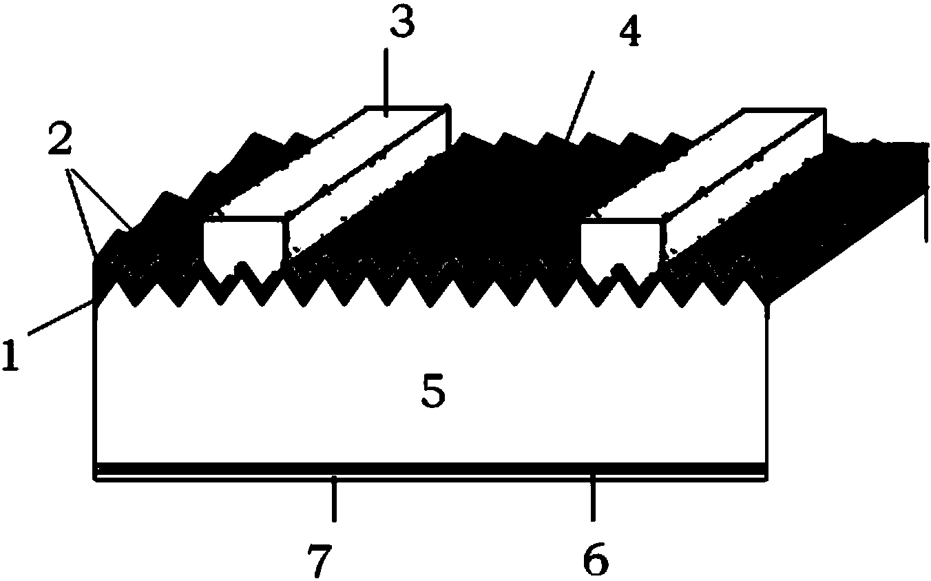
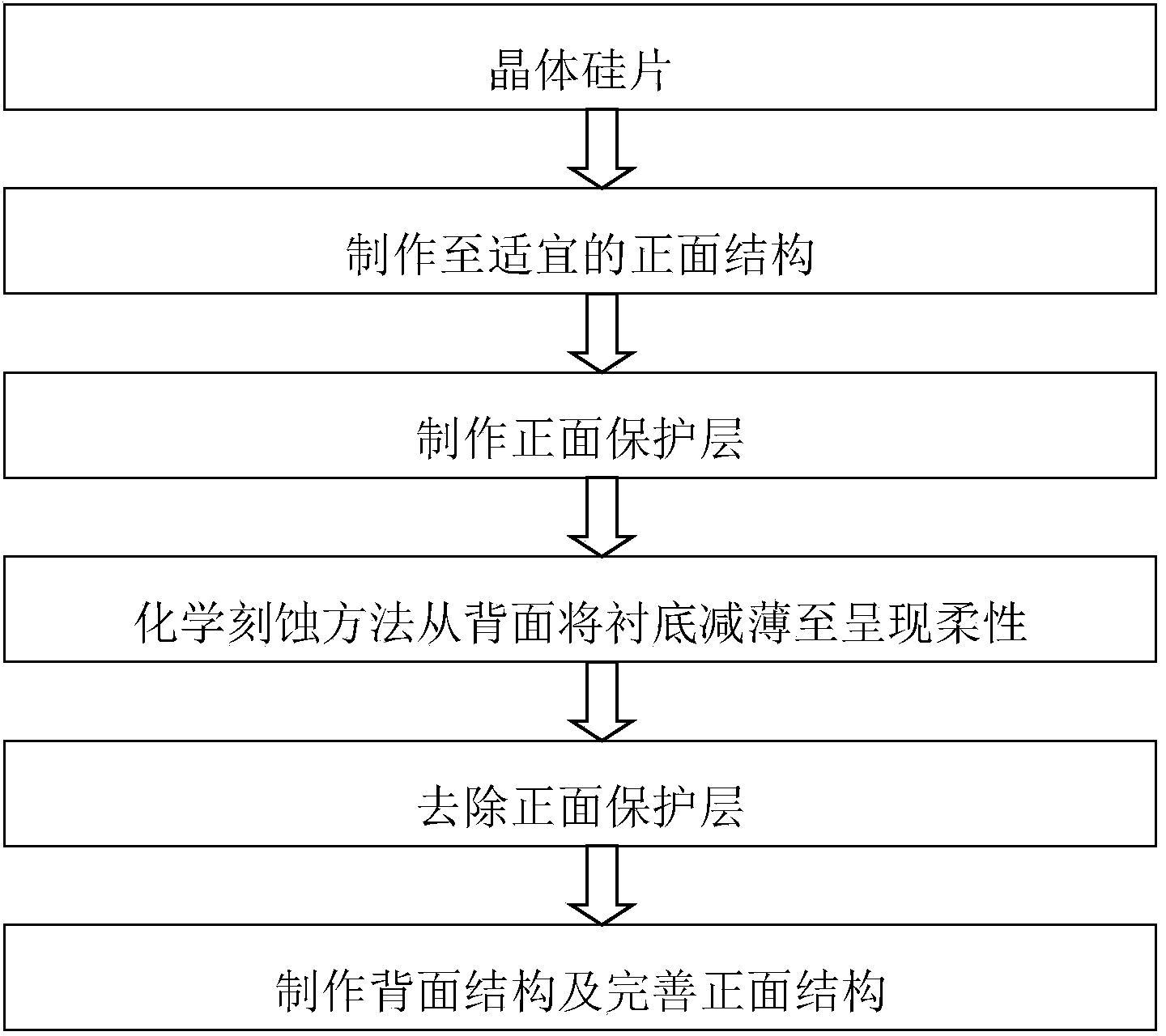
[0019] 1) A p-type monocrystalline silicon wafer with a thickness of 200±20um and a resistivity of 1-3Ω·cm is used as the substrate.
[0020] 2) Using conventional non-flexible crystalline silicon cell technology, the substrate is textured and actinized, thermal diffusion is formed to form an n-type emission region, the edge n-type layer is removed by plasma dry etching, PSG is removed, and SiNx is passivated by PECVD deposition on the front side Anti-reflection layer, screen-printed silver electrodes on the front, and baked and sintered silver electrodes on the front.
[0021] 3) The front side is spin-coated with ~50um PMMA as a protective layer, and baked and cured.
[0022] 4) Using HF+HNO3+CH3COOH solution, the substrate is thinned to ~35um from the back, and the substrate exhibits very good flexibility.
[0023] 5) Remove the PMMA protective layer on the front.
[0024] 6) The metal aluminum layer of ~2um is therma...
Embodiment 2
[0025] Example 2, structure of passivated front and back cells (PERC):
[0026] 1) Use an n-type single crystal silicon wafer with a thickness of 200±20um and a resistivity of ~50Ω·cm as the substrate.
[0027] 2) Using conventional non-flexible crystalline silicon cell technology, the substrate is textured and actinized, thermally diffused to form a p-type emission region, and the back and edge p-type layers are removed by floating acid etching to remove BSG.
[0028] 3) The front PECVD deposits ~400nm SiNx as a protective layer.
[0029] 4) Using NaOH solution, the substrate is thinned to ~35um from the back, and the substrate exhibits very good flexibility.
[0030] 5) Remove the front SiNx protective layer.
[0031] 6) Al2O3 of ~80nm is deposited by ALD on the back side as a passivation layer on the back side.
[0032] 7) Electron beam evaporation on the front side has a grid-shaped silver electrode to form a front electrode, and then ALD-deposits ~80nm Al2O3 on the fro...
Embodiment 3
[0036] Example 3, heterojunction (HIT) crystalline silicon cell structure:
[0037] 1) A p-type monocrystalline silicon wafer with a thickness of 120±10um and a resistivity of 1-3Ω·cm is used as the substrate.
[0038] 2) Using NaOH solution, the substrate is thinned to ~35um from both sides, and the substrate exhibits very good flexibility.
[0039] 3) Deposit ~20nm heavily doped p-type a-Si:H by PECVD on the back to form the back passivation layer and the back field.
[0040] 4) A metal aluminum layer of ~1.5um is thermally evaporated on the back as the back electrode.
[0041] 5) The front PECVD first deposits ~5nm intrinsic a-Si:H, and then deposits ~10nm n-type a-Si:H to form a front passivation layer and a heterojunction.
[0042] 6) Deposit ~70nm TCO on the front side by magnetron sputtering, and electron beam evaporates a silver electrode with grid line pattern on it to form the front side electrode.
[0043] 7) Thermal annealing at lower temperature.
PUM
 Abstract
Description
Claims
Application Information
 - R&D
- Intellectual Property
- Life Sciences
- Materials
- Tech Scout
- Unparalleled Data Quality
- Higher Quality Content
- 60% Fewer Hallucinations
Browse by: Latest US Patents, China's latest patents, Technical Efficacy Thesaurus, Application Domain, Technology Topic, Popular Technical Reports.
© 2025 PatSnap. All rights reserved.Legal|Privacy policy|Modern Slavery Act Transparency Statement|Sitemap|About US| Contact US: help@patsnap.com